


Contents

On-demand webinar
How Good is My Shield? An Introduction to Transfer Impedance and Shielding Effectiveness
by Karen Burnham
When a signal is transmitted, the received signal will always be distorted as a consequence of impedance and other effects. This is why designers work towards minimizing effects on signal integrity.
Designers try to achieve signal integrity by limiting the extent to which electronic noise, inductive coupling, capacitance, and line resistance change the shape and amplitude of the signal. As signal frequency increases, these effects are magnified, and special care is needed to control their undesirable effects in electronic circuitry. Many PCBs now operate at digital signal frequencies of 10 GHz and higher, and this means that appropriate measures are needed to prevent unacceptable signal degradation and their consequential errors.
What is signal integrity in a PCB?
Signal Integrity (SI) signifies the signal’s ability to propagate along PCB traces without distortion. Signal integrity is about the quality of the signal passing through a transmission line. It gives the measurement of the amount of signal degradation when the signal travels from the driver to the receiver. This problem is not a major concern at lower frequencies but is an important factor to consider when a PCB operates at a higher speed and a high-frequency (> 50MHz). In the high-frequency regime, both digital and analog aspects of the signal need to be taken care of.

Signal Integrity eBook
6 Chapters - 53 Pages - 60 Minute ReadWhat's Inside:
- Impedance discontinuities
- Crosstalk
- Reflections, ringing, overshoot and undershoot
- Via stubs
Download Now
When a signal propagates from the driver to the receiver, it doesn’t remain the same, whatever has been sent originally will be received with varying degrees of distortion. This signal distortion happens due to factors, like impedance mismatch, reflections, crosstalk, jitter, ground bounce, and PCB ringing. A designer’s primary aim should be minimizing such factors so that the original signal could make it to the destination with minimum distortion. Special care is also needed to maintain signal quality and to control their undesirable effects in electronic circuitry.

Here, we will discuss the potential signal integrity problems, where they come from, why it is important to understand them, and how we can analyze and resolve these issues. Concerning electrical design, signal integrity should focus on two main aspects; timing and signal quality.
- Does the signal reach its destination within the given time limit?
- When it reaches its destination, is it in good condition?
Several factors contribute to signal degradation. These include the characteristics of the signal, system impedance, propagation delays, attenuation, crosstalk, voltage fluctuations, and electromagnetic interference.
Why maintaining signal integrity is a challenge?
Maintaining signal integrity means to ensure acceptable signal quality within the system.
The rapid technological advancements are making it tough for the system developers to maintain undistorted signals at the receiver. Rising bandwidth is a bottleneck for signal integrity. Today’s electronics need faster bus cycle time, enhanced transaction time (in nanoseconds), and even speedy rise time.
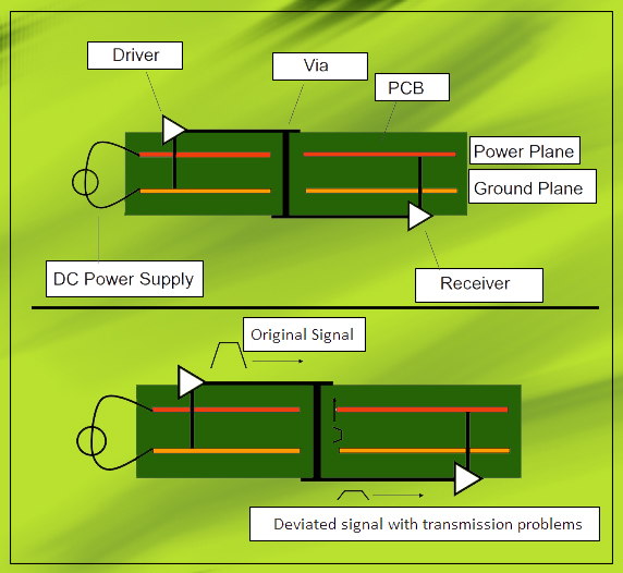
Circuit board’s space requirement also affects signal integrity. PCBs still need sufficient space for IC, connectors, and passive components. This space induces more distance between components and it leads to delays. We all know distance reduces the overall system speed. The circuit board traces act as transmission lines when driven by the signals having rise times of less than four to six nanoseconds. At low frequencies, a trace’s resistive characteristics come at play. On the other hand, at high frequencies, it starts to act as a capacitor and inductance plays a significant role.
To learn the efficient ways to assemble cables and connectors, see the interview assembling connectors and cables for signal integrity with Keven Coates.
What factors are responsible for signal integrity problems?
Factors like characteristics of the signal, system impedance, propagation delays, attenuation, crosstalk, voltage fluctuations, and electromagnetic interference contribute to signal distortion resulting in signal integrity problems.
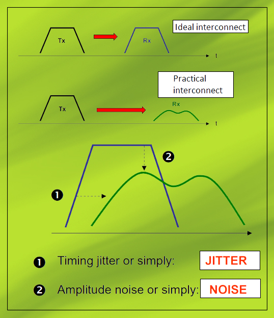
- Signal characteristics: Ideally, a digital signal is a square wave but practically, it takes some time for the signal to switch from one state to another. So, that is the reason, there is always a degree of signal distortion present. The rise time of the signal determines the maximum data transmission rate that is possible and is often measured by evaluating the signal knee frequency. The goal of the circuit designer is to realize a circuit with a flat response at all frequencies up to the knee frequency.
- Interconnect effects: Ideal interconnect only introduces a delay in the signal, but practically, it also changes the timing and amplitude of the signal. This deviation is called jitter and amplitude noise, respectively.
- Impedance: Changes in the impedance that a signal sees cause reflections, ringing, and distortion. The degree of interference intensifies with the increase in the signal frequencies associated with digital circuits. PCB trace branches, line stubs, connector pins, and vias all create impedance discontinuities.
- Propagation delay: Signals that travel different distances or through different mediums do not arrive at their destination at the same time. These discrepancies, called signal skew, cause signal sampling errors, particularly at high clock frequencies.
- Attenuation: The amplitude of a signal is degraded by the resistance of PCB traces and the board’s dielectric dissipation factor. The effect is more noticeable at high-frequency since signals tend to travel along the surface of traces at high frequencies. Attenuation leads to slow signal rise times and increases the possibility of data errors.
- Crosstalk: Rapid voltage and current transitions induce voltages in adjacent traces due to inductive and capacitive coupling. These voltage spikes are known as crosstalk and may cause data errors.
- Reflections: Reflections are caused by termination and board layout problems, where the outgoing signal bounces back toward the source and interferes with the following pulses.
- Ground bounce: Due to excessive current drawn the circuit’s ground reference level shifts from the original. This is due to ground resistance and interconnect resistance such as bonding wires and traces The ground voltage levels at different points in the ground will, therefore, be different. This is known as a ground bounce as ground voltage will vary with the current.
- Supply voltage fluctuations: As devices switch, the flowing current generates a voltage drop in supply and ground rails. This, in turn, leads to fluctuations in the supply voltage at each device, and the cumulative impact creates noise and may result in high bit error rates.
- Electromagnetic Interference (EMI): Every switching operation creates a certain amount of noise, and its intensity is magnified because devices switch at the clock frequency. This noise can be radiated by traces acting as an antenna. The strength of the radiated signal is proportional to the switching frequency and may cause unwanted interference.
To get some valuable insights into the signal integrity challenges in high-density circuit boards, read 10 HDI PCB design tips to maintain signal integrity
What are the basic ways to solve signal integrity problems?
Signal degradation must be minimized by targeting the factors that contribute to signal interference because their collective effect significantly decreases the stability and reliability of high-speed digital circuitry. Proper understanding of signal integrity problems will help you to treat them in advance and it will also mitigate the chances of their occurrence in the further project cycle. Here are some guidelines for improving signal integrity in a PCB.

High-Speed PCB Design Guide
8 Chapters - 115 Pages - 150 Minute ReadWhat's Inside:
- Explanations of signal integrity issues
- Understanding transmission lines and controlled impedance
- Selection process of high-speed PCB materials
- High-speed layout guidelines
Download Now
- Impedance matching: At digital circuit frequencies, signal lines act like transmission lines, and the impedances of the source, receiver, and signal traces should be matched to minimize the reflections. PCB trace termination techniques may be used, the length of stub traces should be reduced and devices should be daisy-chained. Keep signal lines short and use wide return paths.
- Minimize the effects of propagation delay: Signal skew can be minimized by matching the length of signal traces.
- Reduce signal attenuation: The use of low-loss dielectric materials and low resistance traces will minimize signal attenuation.
- Reduce crosstalk: Maximize the distance between signal traces and use ground planes. Don’t split the return paths, and use low dielectric material in the PCB construction. Consider using differential signaling, which is less sensitive to the effects of crosstalk.
- Minimize supply voltage fluctuations: The use of power and ground planes mounted on the outer PCB layers and covering as much surface area as possible will reduce volt drops. It also helps to keep all leads short and to use multiple decoupling capacitors placed close to the device power pins.
- EMI reduction: Use a ground plane, or route the signal return line under the signal line, to minimize the loop area that may radiate radio frequencies. Also. keep trace inductances low to limit radiofrequency radiation. Read more about PCB EMI design guidelines here.
How to test/check for signal integrity?
Signal characteristics observations and measurements become easier when we use the right tools. Logic analyzers, oscilloscope, and spectrum analyzer can be used to measure signal deviations. Such measuring equipment can be used to launch distorted signals for stress testing to evaluate the efficiency of new devices and systems. They also provide missing system inputs. A time-domain reflectometer can also be used for tracking signal path impedance variation problems that cause reflections or amplitude loss.
A good SI testing tool should contain 2D field solvers for extracting impedance and capacitance matrices of single/coupled transmission lines and single/coupled lossy transmission line simulator. It should also contain 3D field solvers for wire bonds, vias, metal planes, and behavior modeling of drivers and receivers. Such tools should also take physical layout files as input data and provide simulation results in both the time and frequency domain.

What is an eye diagram in signal integrity?
The eye diagram is a shortcut to detect signal integrity issues. This visual tool gives us a graphical representation of how a channel degrades the signal. It lets you see any signal line as an eye diagram. It represents all possible positive and negative transitions and both data states on a single screen. This overall image looks like an eye that’s why it’s called an eye diagram.
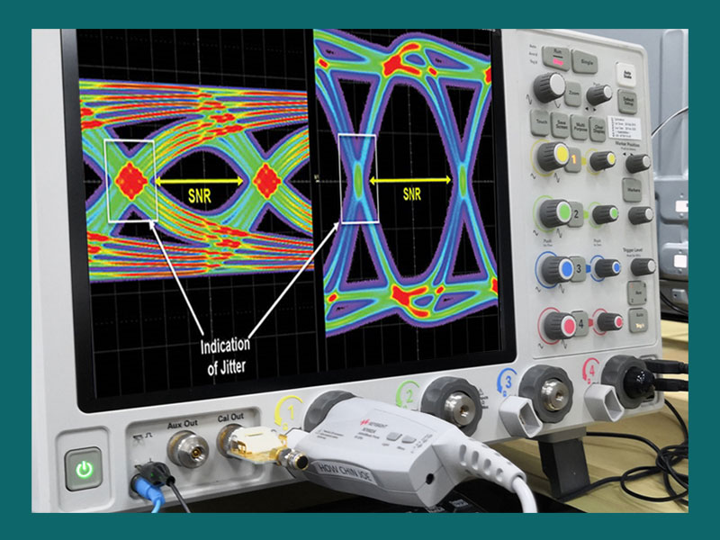
Ideally, a new trace should align itself perfectly with the previous traces. But in reality, the composite image appears blur due to signal integrity factors, where jitter causes blur in the horizontal direction while noise causes blur in the vertical direction. It helps the designers to identify problems like slow rise times, inter-symbol interference, and attenuation levels.
Signal integrity analysis
To initiate the signal integrity problem analysis, we will be requiring various techniques to check signal integrity.
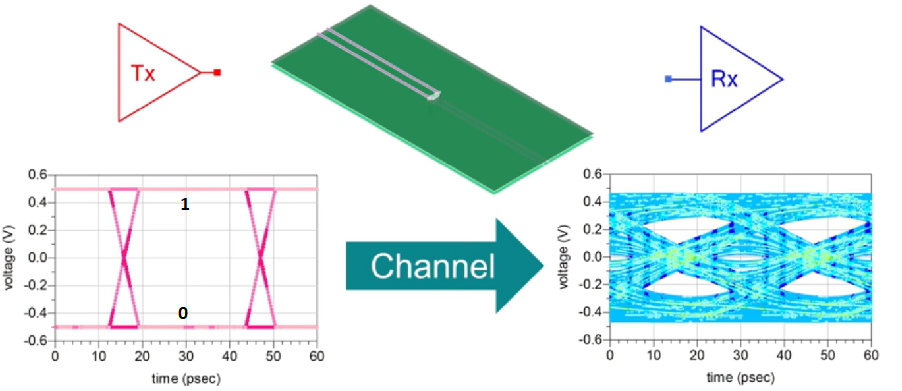
- Channel simulation: We have a channel that constitutes a Transmitter, a Receiver. The eye diagram tells us the extent to which the channel degrades the transmitted signal. As we can see in the image, on the Tx side, the eye is open, and the ‘0’ and ‘1’ levels can be spotted easily. When the signal traverses the channel and reaches the Rx, the eye is almost closed, and it is tough for the receiver to differentiate a ‘0’ from ‘1’. And, this is the point where we know that the signal integrity problem is prevailing.
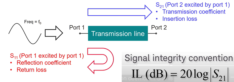
- Identifying the root cause of signal degradation: Next step is finding out the root cause of degradation using mixed-mode S-parameter analysis and time-domain reflectometry. Let us consider a transmission line section and send a sine wave having frequency f0 at port S11. S11 is a reflection coefficient and is related to return loss. It tells us how much signal is reflected back out of port 1. The parameter S21 tells us how the transmission line transmits the signal. S21 is a ‘transmission coefficient and it is related to insertion loss.
Now, the question is when we can use mixed-mode S-parameter analysis? These parameters are used, whenever, we use a pair of transmission lines to transmit a differential signal from differential port 1 and 2. The mixed-mode parameters tell us how the transmission reacts to differential and common signals.
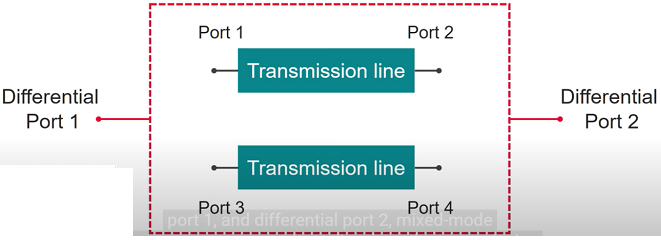
SDD11: Differential output at port 1, excited by Differential input at port 1.
SDD11: Related to differential return loss.
SDD21: Related to differential insertion loss.
SCD21: Mode conversion: EM generation.
SDC21: Mode conversion: EM susceptibility.
Where the term DD gives information about differential responses while the term CD provides information about how much common signal is generated by differential input signals. Also, the term DC tells how much differential signal is generated by common input signals.
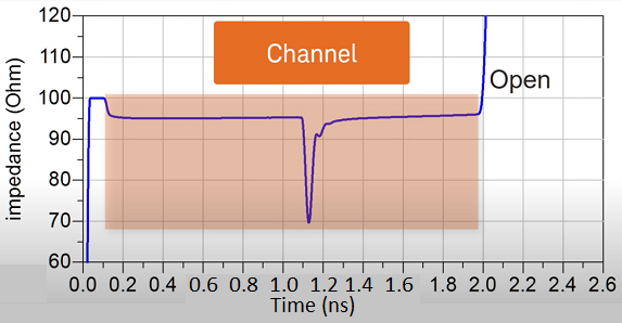
Since s-parameters give the frequency response of the channel, we use time-domain reflectometry to deduce spatial and timing information. On the TDR plot, the right-hand side showcases the ‘open’ circuit to help us identify the end of the channel.
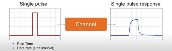
- Explore design solutions: Here, we are exploring the design solution by considering the single pulse response. We send a single pulse with a specific time and data rate to evaluate the single pulse response at the output.
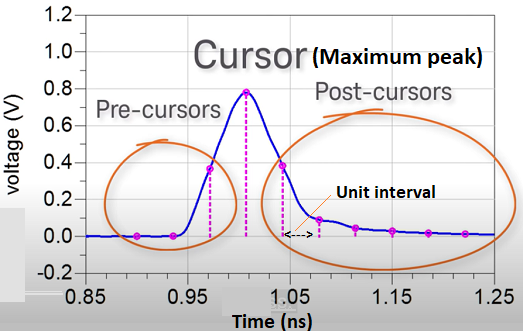
Let us have an example of a single pulse frequency response. If we start from the maximum peak of the response and name it as ‘cursor’ then we can create a cursor diagram by dividing the response based on unit intervals. The cursor diagram tells us how many pre-cursors and post-cursors the pulse response is spreading across. The amount of spreading also gives information about intersymbol interference.
Signal integrity analysis from the perspective of the electromagnetic field
In digital prospect, identifying signal integrity problems at the logic level is an easy task in comparison to a circuit and electromagnetic field (EM) level. The majority of the SI problems are EM problems in nature, be it reflection, crosstalk, or ground bounce. That’s why understanding the physical behavior of SI problems from the EM perspective is very good. For example, in a multi-layer PCB, a switching current in via ‘A’ will generate EM waves that propagate away from the via following the radial direction between the metal planes. The fields developed between the metal planes will create voltage variations between them. When the waves approach other vias, they will induce currents in those vias. And the induced currents will, in turn, generate EM waves propagating between the planes.
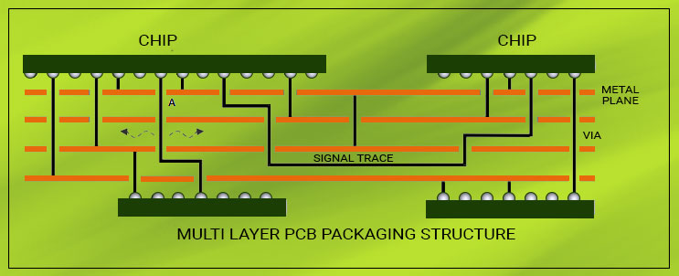
As soon as these waves reach the edges of the package, a part of them will radiate into the air while the other part will get reflected back. When the waves bounce back and forth inside the PCB packaging structure and superimpose each other, resonance will occur. Wave propagation, reflection, coupling, and resonance are the typical EM phenomena that happen inside a packaging structure during signal transients. Though EM analysis is more accurate than circuit analysis, it includes complex algorithms. This is the reason why SI analysis is performed using circuit simulators.
To know more about signal integrity analysis, read our article Unlock Your Signal Integrity Analysis Potential.
Transmission line theory emerges as a boon for today’s SI analysis. Signal’s rise time is a critical parameter in SI issues. In SI analysis, the electric models for various interconnects can be treated as transmission lines. It is essential to by heart the basics of transmission line theory and to understand the transmission line effects in high-speed PCB design.
A good PCB layout and design is a complex task with many challenges. Special attention must be paid to ensure the line impedances are carefully matched and the discontinuities are avoided. Low-loss PCB dielectric materials should be chosen to limit stray capacitances. The use of ground and power planes goes a long way toward minimizing noise by limiting power supply fluctuations, reducing inductive coupling, and avoiding EMI.

Controlled Impedance Design Guide
6 Chapters - 56 Pages - 60 Minute ReadWhat's Inside:
- Understanding why controlled impedance is necessary
- Stack-up design guidelines
- How to design for impedance
- Common mistakes to avoid
Download Now


