PCB X-ray inspection, also known as automated X-ray inspection, is a quality monitoring method that finds hidden defects in a circuit board. This technique is widely used in medical and aerospace sectors to find out hidden features and to identify errors such as solder bridges, solder shorts, etc.
What is PCB X-ray inspection?
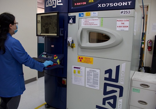
Automated X-ray inspection (AXI) is the widely used method to determine invisible defects related to ICs (CSP:chip-scale package) and BGAs in printed circuit boards. This system uses an X-ray as a scanning source. It is suitable for detecting large voids and cracks. This method can access internal geometries and structural compositions in a non-destructive way. AXI works in the same manner as AOI by capturing images. The only difference is AOI uses a light source while AXI uses an X-ray for scanning.
All the SMDs and their solder joints can be examined by X-ray inspection. The machine’s software creates real-time 2D images of components. It is easy to visualize and analyze defects with the help of those images. The equipment can also find out the root cause of each issue.

Design for Testing Handbook
7 Chapters - 28 Pages - 45 Minute ReadWhat's Inside:
- PCB testing strategies
- Guidelines to design and place a test point for FPT
- Directives to make your board ICT compatible
- Benefits and drawbacks of various testing methods
- Defects that you can identify through board testing
Download Now
How does the X-ray inspection system work?
Generally, materials absorb X-rays in proportion to their atomic number, density, and thickness. Heavy materials absorb more X-rays compared to lighter materials. Such heavy materials appear darker in their images than those absorbing very few X-rays. Lighter materials are more transparent to this radiation.

As shown in the above image, the dark black area represents a material made of heavy elements whereas the transparent or comparatively light area represents a material composed of light elements. This shows, X-ray inspection is effective in determining hidden problems such as opens, shorts, misalignment, and missing electrical components.
Talking about PCBA, solder joints are made of heavy materials, and other parts such as packages, silicon ICs, and component leads are made of light materials. Hence, high-quality solder joints look darker on images than other parts.
AXI machine consists of three parts:
- X-ray tube: This tube generates X-rays. It has two types: open tube and closed tube. The type is selected based on the correspondence to the resolution of the inspection device. As the resolution increases, intricate/delicate details will be more visible. Generally, for BGAs and CSPs 2 μm resolution is required.
- Sample operation platform: A sample operation platform can move to inspect the sample from various angles and magnification. It is possible to examine the sample through an oblique angle.
- Detector: A detector can capture X-rays passing through the sample and transform them into a visual representation (projections) that can be understood by users.
This board inspection method is carried out with an X-ray projection microscope. Firstly, the radiation launching tube generates X-rays by passing through PCBs subjected for inspection. As stated earlier, materials have different X-ray absorption capacities as per their atomic number. Therefore, the projection also differs. The higher the material density, the deeper will be the shadow and vice versa.
Hence, X-ray inspection systems should have clear X-ray images that offer the correct information during defect analysis. To achieve this, AXI should have enough magnification.
Choosing the right inspection method
There can be confusion while selecting inspection methods (AOI and AXI) for classifying defects. The following charts give an idea for selecting the appropriate method
| Soldering defects | AXI | AOI |
|---|---|---|
| Open circuits | Yes | Yes |
| Solder bridges | Yes | Yes |
| Solder shorts | Yes | Yes |
| Insufficient solder | Yes | Yes |
| Solder void | Yes | No |
| Excess solder | Yes | Yes |
| Solder quality | Yes | No |
| Component defects | AXI | AOI |
|---|---|---|
| Lifted lead | Yes | Yes |
| Missing component | Yes | Yes |
| Misaligned/misplaced component | Yes | Yes |
| Incorrect component value | No | No |
| Faulty component | No | No |
| BGA and CSP defects | AXI | AOI |
|---|---|---|
| BGA shorts | Yes | No |
| BGA open circuit connections | Yes | No |
Automated X-ray inspection is a tool that enhances the quality of printed circuit boards. It can identify and prevent failures quickly, which in turn saves both time and unnecessary expenses.


