When arranging the stack-up of a circuit board, the manufacturer should clearly understand the order and orientation in which the layers are to be placed. Even though the PCB stack-up design clearly defines each and every layer and its order, there should be physical labels on each layer for their accurate placement. Otherwise, there is a chance of the operator messing up the layer order. Let us have a look at the important guidelines that should be followed to get the correct layer orientation.
What is a PCB layer?
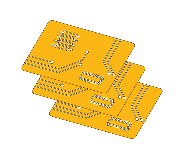
A circuit board is constructed by laminating many layers together. There are substrate layers, copper layers, prepregs, etc. All of these layers are combined to form a stack-up. The number of layers needed is determined by the output requirements of the board.
What is layer orientation in PCBs?
While arranging the layers in a circuit board, the manufacturer needs to have an idea about the order and orientation of each layer. Be it, single-layer or multi-layer boards, a physical label on each layer is important to avoid mistakes. Therefore, there should be a label etched on them for clarity. This helps to position all the layers in the design. This is called layer orientation in PCBs.
Why is PCB layer orientation required?
The question that arises in our minds is if the design software has all the layers properly oriented and ordered, then what is the need for physical labels? The answer of course is to conveniently place the layers and support visual inspection. When the layers are properly labeled, a simple visual inspection can identify the errors in order and orientation. This ultimately helps in proper component placement.

PCB Design for Assembly Handbook
6 Chapters - 50 Pages - 70 Minute ReadWhat's Inside:
- Recommended layout for components
- Common PCB assembly defects
- Factors that impact the cost of the PCB assembly, including:
- Component packages
- Board assembly volumes
Download Now
How to label the board layers?
The process of labeling has a universal standard. It should be done as per this specific standard to avoid miscommunication.
The top layers are usually marked as TOP and the bottom layers as BOT (in a mirrored form).
These labels, just like the traces, are subject to design rule considerations.
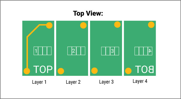
If the board is multi-layered, then the inner layers along with the top and bottom layers are labeled. This labeling is done with numbers. These numbers are enclosed in a square box. This reveals which inner layer has to be placed first after the top layer and so on. Each square box with the layer number should be placed a little bit offset to the previous layer’s box. This is done so that when we view it from the primary side, it looks like a long rectangle with all the consecutive layer numbers in order. The solder mask around this feature should have a clearance of at least 100 mils.
Stacking stripes
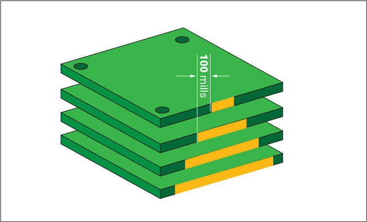
Stacking stripes are copper stripes that are initially 200 mils long and 50 mils wide, placed on the edge of the layers.
As we go down the stack-up, the length of the stripe is increased by 100 mils on each layer. This is to indicate the difference in layers and their consecutive order in the stack-up. So when viewed from the edges, the stripes increase in length as we descend down the stack-up and assure the correct order of the layers.
Hence, we can understand that even though the design software has all the layer labels, it is necessary to physically label every layer of a circuit board. This will help the fabricator to avoid any errors related to layer orientation.


