Before manufacturing a PCB, engineers lay down the board design based on the end application requirements. PCB design engineers employ electronic design automation (EDA) software, also referred to as electronic computer-aided design (ECAD) software, to create a blueprint of the desired circuit board. This requires an in-depth knowledge of the platform architecture and a good understanding of the associated libraries. The produced design pattern must be in compliance with the IEEE EMC standards. Later, this design is brought to life (put into production) by a PCB manufacturer.
What are the steps involved in PCB designing?
A board design process is an amalgamation of three main steps:
Design phase
- Circuit block diagram: It involves drawing a conceptual block diagram which is then developed into schematic designs using CAD software.
- Component selection: It concerns selecting components based on the electrical requirements of the end application.
Schematic entry
- Symbol generation: The symbol generation process involves drawing the body of the component, adding pins and pin numbers, defining the reference designators, and assigning a footprint.
- Circuit connections: Next step is tracing out the connections in the circuit.
- ERC checks: ERC checks include pin numbering and label verification for all the components along with component value, polarity, ground pin separation checks, etc.
- Netlist generation: The netlist is generated when the schematic design is complete and ready to be imported into the layout. It is recommended to manually verify the nets to avoid design errors.
- BOM generation: BOM is generated to provide all the inputs in the tools while creating or importing components from the library. The inputs could be MPN (Manufacturing Part Number), package, vendor name, vendor part number, etc.
Layout phase
- Stack-up design: The stack-up design is used as a reference to set up the stack-up in the layout tool. The stack-up design includes deciding the thickness of the board, the number of layers, impedance traces on each of the layers, and the material to be used. All these parameters are entered into the stack-up design tool and the trace widths are calculated for different layers.
- Constraint settings: Constraint settings implements design rules for electrical, physical, and spacing requirements for a layout.
- Board outline: The shape of the PCB is referred to as the board outline and is essentially a closed contour. It can be defined manually and from selected objects.
- Component placement: The component placement process begins by placing the components which are at fixed locations as per the design requirements such as connectors. The next step is to place the main components such as the CPU, memory, and analog circuits. The third step is to place the auxiliary components such as crystals, decoupling capacitors, and series resistors.
- Routing: Routing is defined by placing tracks, arcs, and vias on the copper layers to establish a connection between the two nodes.
- DRC checks: DRC is a process of checking both the logical and physical integrity of a design. These checks are made against all the enabled PCB design rules.
- File generation: The last step is to generate production files such as Gerber, ODB, etc. required by a manufacturer.
What are PCB design tools?
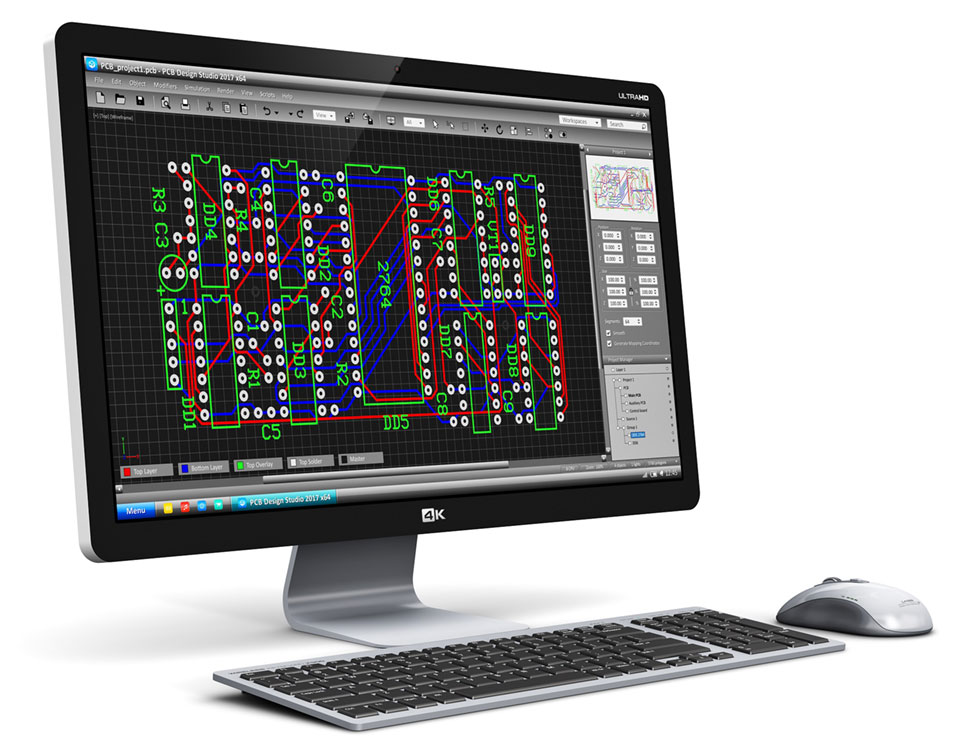
PCB design software tools are used to define electrical connectivity between the components on a manufactured circuit board. They create schematics, BOMs, netlists, and PCB layouts.
A Board schematic tool has the following features:
- Symbol generation
- Symbol libraries
- Net connections
- ERC error checking
- Netlist and BOM generation
A PCB layout tool features:
- Constraint settings
- Board outline generation
- Defining the number of layers
- Component placement
- Routing of nets with special features of differential pair routing length matching
- DRC checking
- File generation for manufacturing
Circuit board design (EDA) tools must have the above-mentioned features.
Designers can use the software for pulling component footprints from libraries, followed by verification of their respective schematic diagrams. Here are some of the commonly used EDA tools available:
- Altium Designer
- Cadence Allegro Orcad
- Mentor Graphics pads and expedition
- Cadstar
- Zuken
- KiCad
- EAGLE
- SOLIDWORKS PCB
The prime factors to consider while choosing a PCB design software are:
- User interface (UI)
- Price
- Features
- Large components libraries
- Routing features
Top EDA tools best for PCB design
The automation software programs establish a convenient approach to PCB designing that can be easily transformed into a physical PCB. An aspiring PCB designer should gain hands-on experience with some of the popular design tools like Altium Designer, Eagle, and OrCAD, as listed below.
Altium Designer
Altium Designer is used for designing electronic products including circuit boards for the automotive, aerospace, defense, and telecommunication industries.
It is an advanced CAD tool that provides a complete PCB design environment. This designer tool features a modern UI and interfaces with third-party analysis, synthesis, and 3D mechanical software.
Cadence OrCAD
OrCAD automation tool provides the functionalities and capabilities of board design. It incorporates a user-friendly interface and features real-time board design, high-speed signal routing, DesignTrue DFM, and interactive 3D. Orcad provides the following products:
· Schematic editor (OrCAD Capture)
· Analog/mixed-signal circuit simulator (OrCAD EE PSpice)
· PCB board layout solution (OrCAD PCB Designer)
Cadence Allegro
Allegro Cadence is a designer tool that is suitable for large enterprises, complex projects, and low-performance hardware. This tool works fine even when installed on machines with 512 MB of RAM. The Allegro Cadence software is scalable and contains everything needed to create a board layout with a fully integrated design flow. This software addresses technological and methodological challenges while making the design cycles shorter and more predictable.
Mentor Graphics PADS
Mentor Graphics PADS is a PCB software that incorporates built-in DFF, automatic routing and high-speed interactive routing, and 3D visualization and placement. Mentor Pads software offers schematic design, analog/mixed-signal circuit simulation, and simulation and analysis. This software reduces design time through integrated design entry, constraint management, 2D/3D board layout, and analysis and verification.
Zuken CADSTAR
Zuken’s CADSTAR PCB design software offers a complete design environment. CADSTAR offers design capability throughout the design flow starting with the schematic through layout, routing, signal integrity simulation, power integrity analysis, and 3D mechanical integration.
The primary goal is to realize accurate and precise routing plans. The design software could be the same but not the routing strategy as it depends on the designers’ problem-solving skills.
Autodesk Eagle
Eagle (easily applicable graphical layout editor) is a designer tool for drawing electrical circuits and traces. The package comes with three modules: schematic editor, PCB layout editor, and auto-router.
KiCad
KiCAD is an open-source, cross-platform designer tool utilized to create design schematics. This software comes with schematic capture, a PCB layout, and a 3D viewer. This tool can be used to create up to 32 layers of copper.
KiCad Design Guide
10 Chapters - 161 Pages - 180 Minute ReadWhat's Inside:
- Creating a component symbol library
- Setting up board parameters and rules
- How to route differential pairs
- How to place of components


