Speak to an Account Manager
![]() +1 (800) 763-7503
+1 (800) 763-7503
What is flying probe testing for PCB assembly?
Flying probe testing, an integral facet of PCB assembly, employs test probes that traverse the board, detecting defects in a dynamic and efficient manner. At Sierra Circuits, we leverage the advanced capabilities of Seica Spa Pilot V8 machines for flying probe testing.
The flying probe tester can test for shorts, opens, and component values such as resistance, capacitance, and inductance.
A notable advantage of flying probe testing lies in its fixtureless nature during in-circuit testing, eliminating the need for custom fixtures. This not only expedites the testing process but also contributes to its cost-effectiveness, making it an ideal choice for prototype development and low to mid-volume production. The absence of custom fixtures streamlines the testing workflow, enhancing the adaptability of flying probe testing to diverse PCB assembly requirements. This amalgamation of advanced technology, versatility, and cost-effectiveness positions flying probe testing as a cornerstone in ensuring the quality and functionality of boards in various production scenarios.
How we test your PCB assembly
We start by generating a test program which is loaded into the flying probe tester. The circuit board assembly to be tested is then placed on a conveyor belt so that it can move inside the testing area where the probes are present.
When our engineering team runs the test program, the probes will contact the component pads, test pads, and the unmasked vias as per the pre-loaded test program. The tester will apply electrical test signals and power to the probe points and make measurements.
These measurements will be processed inside the tester to find if the circuit portion between the probes is delivering the expected results within the specified tolerances. This is how we detect the defective units.
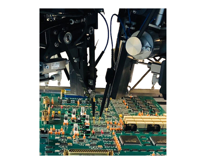
Inside a probe testing machine
The flying probe tester hardware includes signal generators, DC and AC power supplies, and various sensors. These provide signals required to excite the PCB nodes and make measurements on the component nodes and interconnections and the assembled circuit.
The hardware also includes a camera that automatically inspects component polarity.
Speak to your account manager today to add flying probe test to your order.
Flying probe testing requires ODB++ or IPC-2581 files.
Product Promise
We recommend flying probe testing to customers developing very dense and complex boards. This is our preferred method to test the quality of your PCBA and ensure we can reduce your time to market as much as possible.
Why flying probe testing for PCB assembly?
Not only is flying probe testing cost-effective for small to medium production runs, it also helps R&D teams to go to market faster by ensuring the viability of their electronics right out of PCB assembly.
Testing the inaccessible
As opposed to in-circuit testing that uses pogo pins, a flying probe tester is equipped with fine probe points capable of accessing much smaller pads.
Flexible testing
Because the probe movements and landing positions are generated by software, we can easily reprogram them to apply different testing strategies.
More coverage
By accessing component pins directly through automated probing without requiring specifically built test points, flying probe testing for PCB assembly offers better test coverage than ICT.
Trusted by innovators
Engineers and PCB designers at the world’s most innovative companies choose Sierra Circuits for the highest quality one-stop PCB assembly services, right here in the USA.


Fully assembled PCBs that work the first time. Ready to ship in as quick as 24 hours.
Whether you’re an aerospace engineer or a research and development designer on a tight deadline, Sierra Circuits helps you build electronics with zero defects by offering flying probe testing options that inspect your prototype assembled boards.
IDEAL FOR:
- Small to medium production runs and other R&D teams who need to go to market fast
- Designers and engineers developing very dense and complex boards


Manufacturing Equipment at Sierra Circuits
Our 70,000 sqft state-of-the-art campus in the heart of Silicon Valley contains the most advanced equipment required for the manufacture and assembly of your PCBs. Whether you’re looking for standard quick turn PCBs or boards with the tightest tolerances, made from exotic metals, there’s a reason Sierra Circuits leads the industry in quality and performance.


Fabrication, Procurement, & Assembly. PCBs fully assembled in as fast as 5 days.
- Bundled together in an entirely-online process
- Reviewed and tested by Engineers
- DFA & DFM Checks on every order
- Shipped from Silicon Valley in as fast as 5 days

Fabrication. Procurement & Assembly optional. Flexible and transparent for advanced creators.
- Rigid PCBs, built to IPC-6012 Class 2 Specs
- 2 mil (0.002″) trace / space
- DFM Checks on every order
- 24-hour turn-times available

Complex technology, with a dedicated CAM Engineer. Stack-up assistance included.
- Complex PCB requirements
- Mil-Spec & Class 3 with HDI Features
- Blind & Buried Vias
- Flex & Rigid-Flex boards