What is mixed PCB assembly?
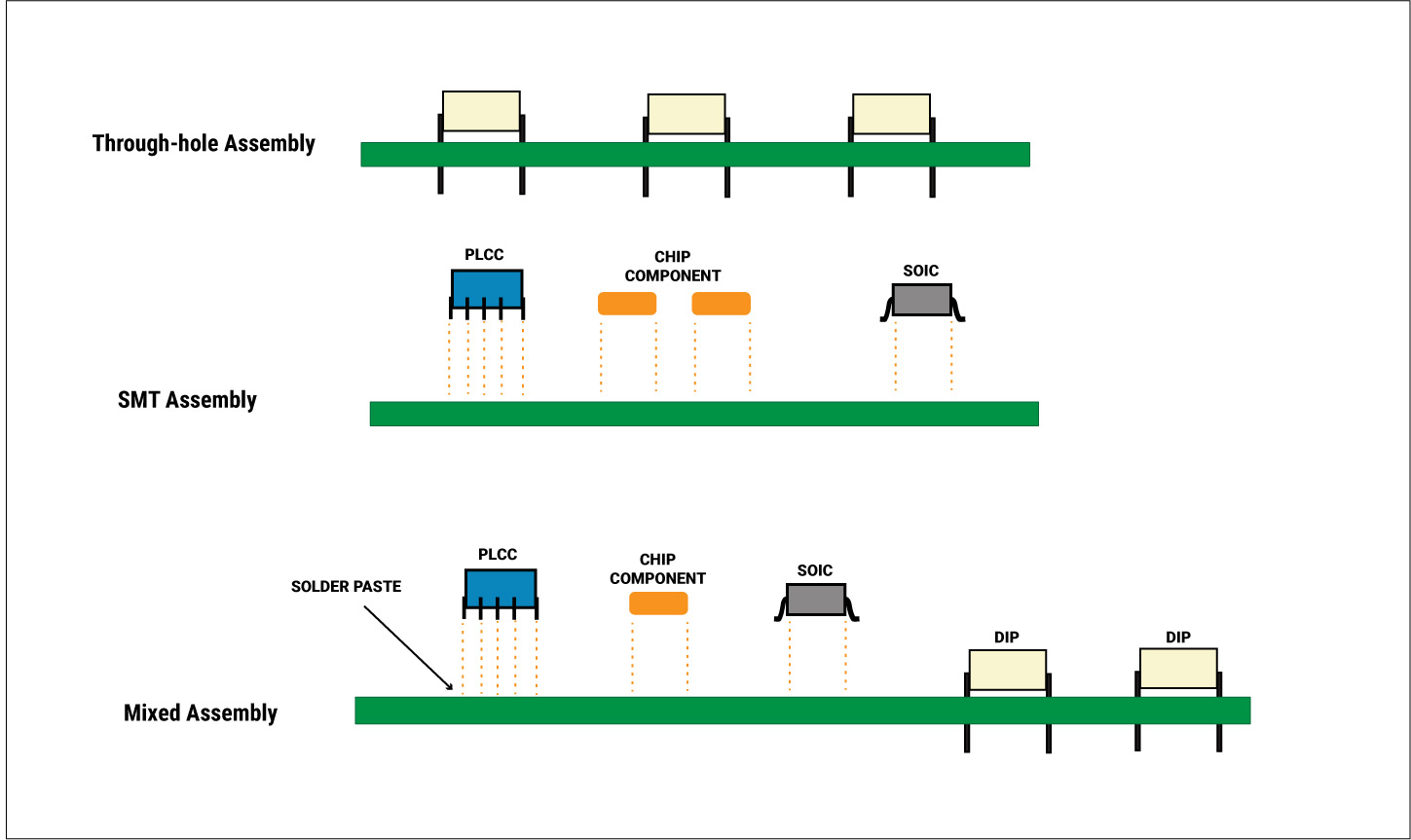
Mixed circuit board assembly includes surface mount devices (SMD) and through-hole components. It brings out the combined advantages of both mounting technologies. Most of the applications incorporate SMD and through-hole components.
What are the mixed assembly advantages?
Mixed assembly features the following advantages:
- 100% inspection using X-ray technology that helps in installation and rework procedures
- High-reliability
- Lightweight
- Increased stress-tolerance
- High precision
DFA considerations for a mixed assembly
Design for assembly (DFA) provides a foresight pointing out the complexities that may arise before the actual assembly process takes place. Without proper planning, the assembly might not match the actual design requirements. Unlike DFA, design for manufacturing (DFM) does not consider the possible difficulties that may arise during the placement of components. Once DFM is completed, we are just left with a bare board on which the components are to be assembled. Before assembling them, we must decide on the following aspects:
- Types of components used
- Automated/manual placement
- Rules for placement of components

PCB Design for Assembly Handbook
6 Chapters - 50 Pages - 70 Minute ReadWhat's Inside:
- Recommended layout for components
- Common PCB assembly defects
- Factors that impact the cost of the PCB assembly, including:
- Component packages
- Board assembly volumes
Download Now
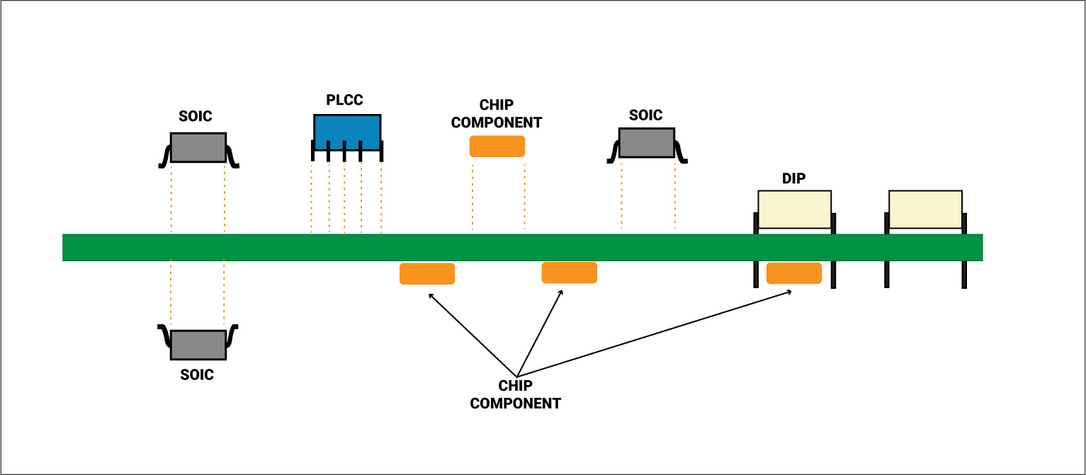
Types of components used
Even though SMDs are used in abundance in PCBs today, there are components that are not suitable for SMT mounting. That is why it is best to apply both technologies on the same circuit board. This ensures all the benefits of SMT like high precision, lightweight, and easier automated mounting along with the THT advantages like robust connections and high stress tolerance.
SMT and THT require different soldering methods. Surface-mount components undergo reflow soldering and through-hole components are subjected to wave soldering/manual soldering.
Automated/Manual placement
The next step is to choose which type of component placement is suitable. Below are the advantages and disadvantages of automated placements.
Advantages of automated placement:
- Fast
- Consistent and accurate
- Reliable and offers high quality
- Low cost for big volumes of the product
Disadvantages of automated placement:
- Lack of precise control while placement
- Not suitable when dealing with low volumes
- Complications may arise with component leads
The above drawbacks should be considered while choosing the method of placement. In the case of fewer batches for assembly, the cost required to set up an automated placement will be high. In such cases, always opt for manual placement.
Design rules for placement of components
While placing components, the following conditions should be met:
- Try to place all components on one side, if possible.
- If the above condition cannot be followed, then try to place the chip-type SMT components on the lower side of the board.
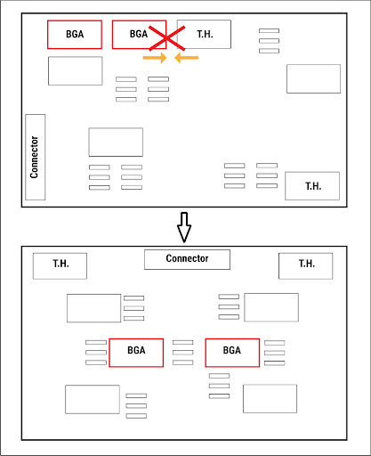
- Never allow two BGA components to face each other.
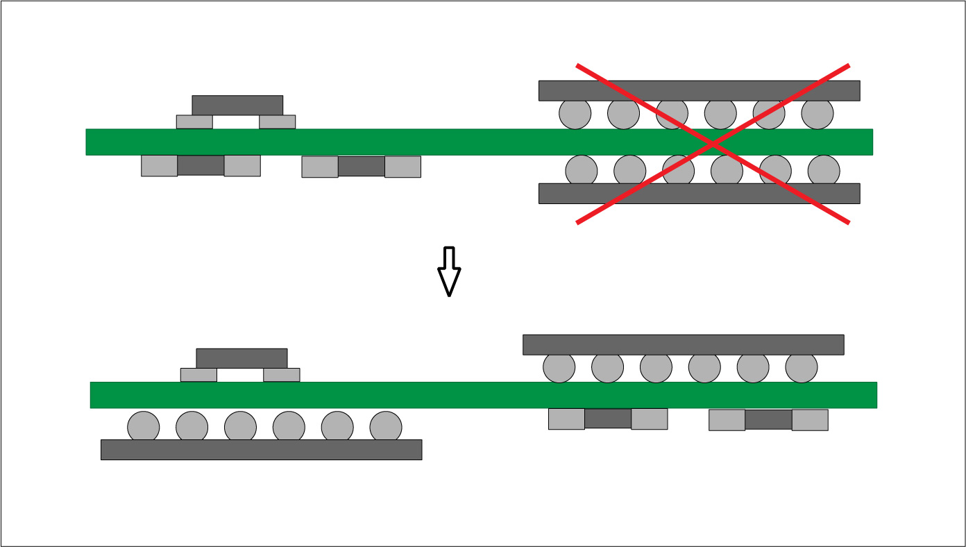
- Always leave a 5 mm gap between BGA components and any passive components on the board. This helps in reballing the BGA if required in the future.
- Try not to place BGA devices and THT components close to each other.
- Always take care of the weight distribution across the board. Large/heavy components should not be placed on the board edges. This will cause bending of the boards.
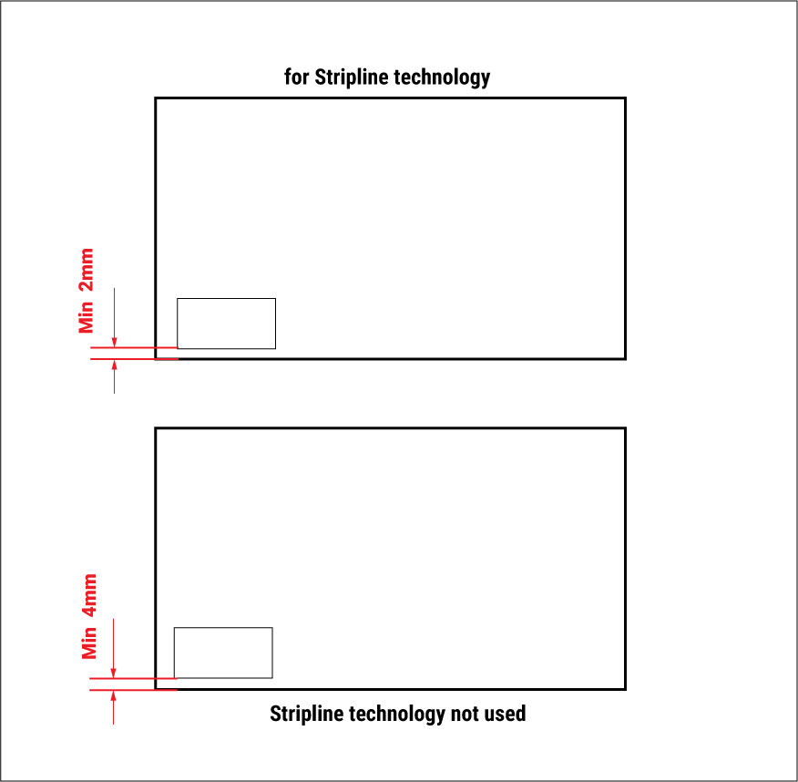
- While using stripline technology, leave a gap of 2 mm between the edge of the board and the components. If stripline technology is not used, then this gap should be 4 mm.
- As much as possible, try and use the same package size. This might not be practical every time but helps to optimize the installation process.
With these aspects in mind, the design for a mixed assembly can be carried out efficiently. A mixed assembly will definitely prove to be more advantageous than opting for a specific mounting technology alone.


