What is the significance of a PCB stack-up?
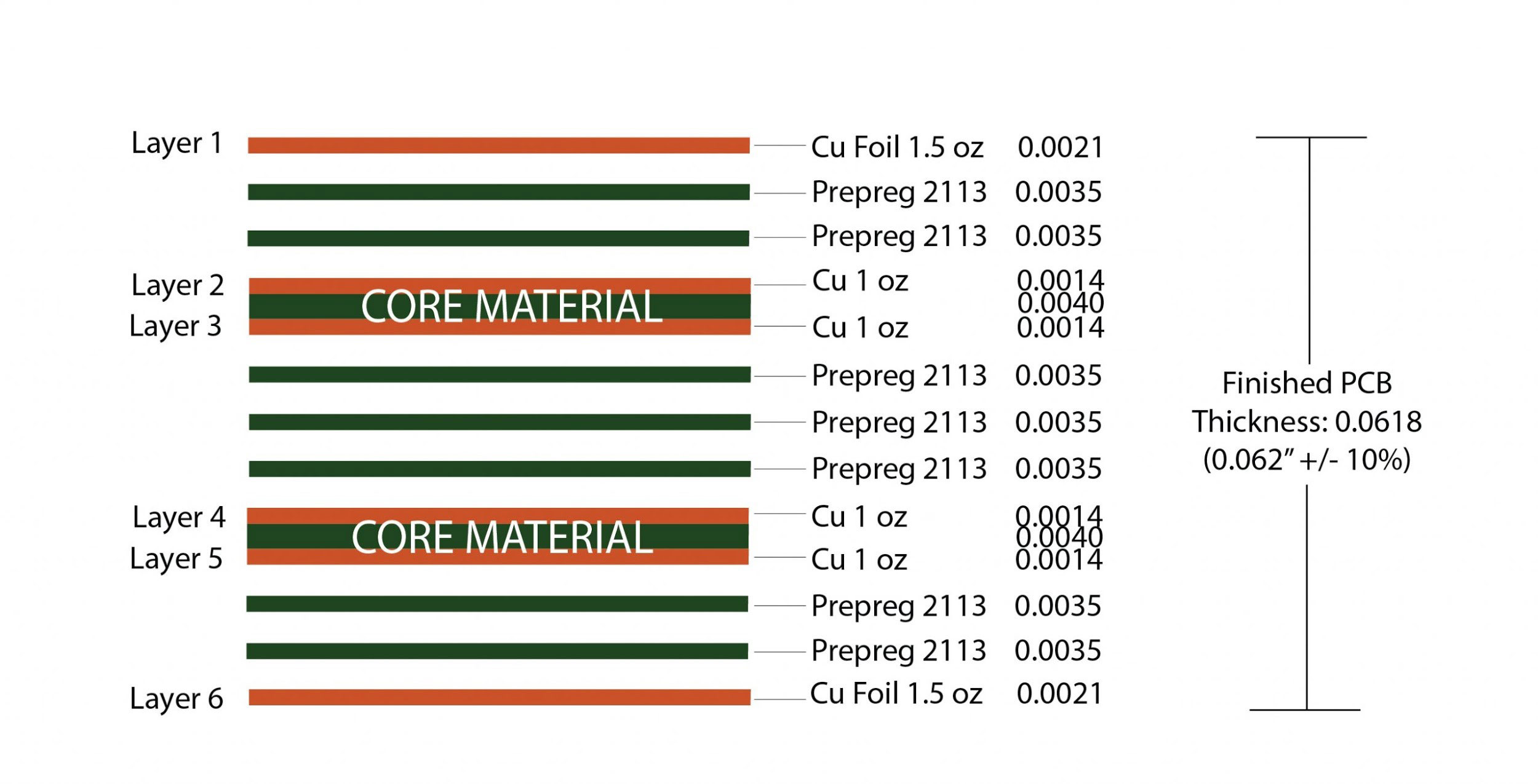
A stack-up describes the construction of a multilayer board in sequential order. It provides vital information like material thickness and copper weights. Stack-ups, also known as build-ups, carry the details of trace width for different controlled impedance traces such as 50 ohms or 100 ohms differential. An ideal 6-layer stack-up is shown in the above image.
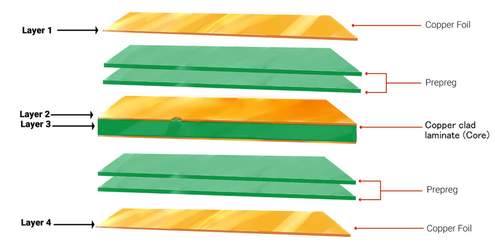
Modern electronic devices have become more complex and require a higher number of circuits and components. It will be a challenging task for the designers to accommodate these complex circuits in a single-layered board. This problem can be tackled by using multilayer PCBs.
What is the standard PCB thickness?
Circuit board thickness is mostly determined by the thickness of copper, materials used, layer count, and operating environment. The standard thickness of a circuit board is roughly 62 mils (1.57mm). Manufacturers, based on the customer’s request, are now fabricating PCBs with two new standard thicknesses, 93 mils (2.36mm) and 125 mils (3.17mm) (150 and 200% of the old standard thickness). Thinner boards of 31 mils thickness can also be fabricated.
HDI stack-up
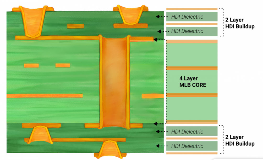
HDI circuit boards have a higher wiring density per unit area than typical PCBs. These boards feature microvias, blind and buried vias, and sequential laminations.
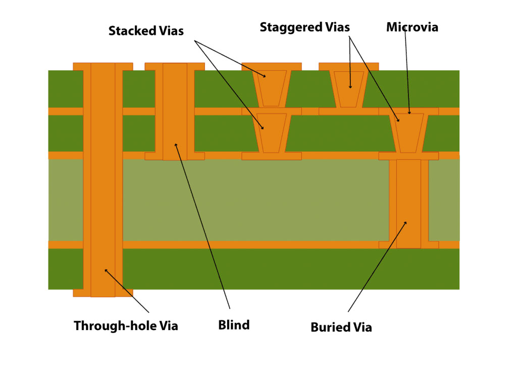
The blind and buried vias can be stacked or staggered.
The HDI build-up architecture follows a slightly different approach compared to the standard stack-up. The number of layers in an HDI board is determined by the number of ball grid arrays (BGA) or highest pin count devices. Other factors affecting stack-up include the number of signal, power, and ground layers.
Some of the prominent HDI board characteristics are:
- Fine trace width ≤ 100 µm
- Microvias of diameter ≤ 150µm
- Capture pads of diameter ≤ 400µm
- Capture pad density of more than 20 pads/cm2
PCB Stack-Up Design Guide
12 Chapters - 55 Pages - 60 Minute ReadWhat's Inside:
- Design guidelines for HDI, flex, and hybrid stack-ups
- Stack-up representation in fab drawing
- DFM checks for layer stacks
- Characteristics of high-speed materials
- Manufacturing tolerances
- PCB stack-up examples with illustrations
Download Now
HDI board materials
Materials for HDI boards should be dimensionally stable and must be easily machinable. These materials undergo laser drills (vaporization) and should be suitable for sequential laminations.
Sierra Circuits recommends FR 370HR and I-Speed materials for HDI PCBs.
Stack-up guidelines for designers
- Always opt for a higher number of layers for PCBs used in high-speed designs and high-power stack-ups, where additional power and ground planes help manage current and heat.
- Ground and power planes enable you to utilize the signal layers exclusively for signal routing. This reduces DC resistance in power and ground layers thereby ensuring fewer DC voltage drops at the devices.
- Signal integrity, or the transmission of signals without distortion, requires a consistent controlled impedance. When the reference plane is missing, the immediate next layer that has a copper feature becomes the reference. This will disrupt the board functionality. Therefore, always ensure there is a reference plane. From the manufacturing standpoint, we need to maintain a consistent etch across the length of the line, both in terms of width and trapezoidal effect.
- Maintain a minimum distance between the power and ground planes for precise layer placement. Other important considerations include avoiding the adjacent placement of two signal levels and constructing a symmetric stack-up of the top and bottom layers.
To learn how proper layer orientation improves signal integrity and reduces EMI, read PCB layer orientation.
- In HDI PCBs, more sequential laminations increase the cost and delivery schedule. Keep the number of sequential laminations to 3 or less.
- The number of planes and signal layers in HDI stack-up should be either odd or even (even is the best for a balanced structure).
- Stacked vias require filling after every sequential layer. This requires more time and an elaborate manufacturing process. Hence, avoid stacked vias if possible and choose staggered instead.
A successful PCB design largely relies on the stack-up. A well-planned stack-up optimizes the circuit board design for better signal integrity, reduced crosstalk, and EMI.


