Flex PCB assembly is the process of assembling components on a flex board. This assembly process is similar to that of rigid boards. Scroll down to learn more about this topic as we answer some of the most common questions.
We are more than your PCB manufacturer. We help you flex your design potential. Get low-to-high volume flex and rigid-flex PCBs manufactured with industry leading quick turnaround times.
Start building a quote online now.
What is a flexible board?
Flex PCBs are built with very thin laminates and exhibit high levels of bendability, tensile strength, and physical flexibility. These boards are also called flex boards, flex circuit boards, and flexible electronics. They can be found in smart watches and medical equipment. Their ability to bend and twist is what makes them distinct from others.
See our FAQ on flex PCBs.
Flexible PCB assembly process
Flex board assembly is the process of assembling components. This process is similar to that of rigid boards. Below image shows the process flow.
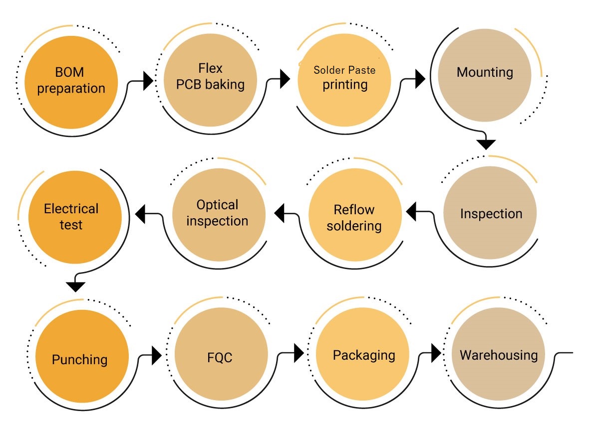
Bill of materials
BOM or bill of materials is a list of components required to assemble a printed circuit board.
Flex PCB baking
A flex circuit board stack-up is set and sent to the baking process to reduce the amount of moisture inside the board. The temperature and duration of the baking process depends on the overall thickness of the PCB.
| Overall thickness of flex PCB | Duration and temperature of baking |
| Upto 1 mm (39 mils) | minimum 2 hours at 120 °C |
| > 1 mm upto 1.8 mm (70 mils) | minimum 4 hours at 120 °C |
| > 1.8 mm upto 4 mm (157 mils) | minimum 6 hours at 120 °C |
Also, see rigid PCB assembly for traditional FR4 board manufacturing and rigid-flex assembly for hybrid designs that combine stability with flexibility.
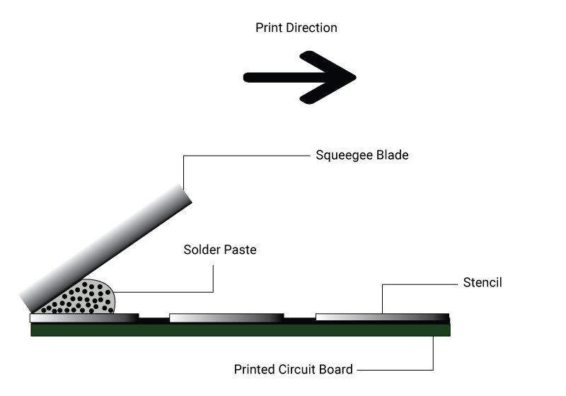
Solder paste printing
Post baking, the board undergoes solder paste printing. In this process solder paste is applied on the PCB surface. The primary goal here is to solder pads onto the circuit board. This is done by screen printing the solder paste through a stencil. A tool called squeegee blade is used to apply the required force on the solder paste to move it across the stencil. Squeegees are generally made of metal or polyurethane.
Silkscreen printing
Silkscreen printing is a process of creating a layer of non conductive ink traces used to identify components, test points, parts of the circuit board, warning symbols, logos and marks, etc. This process is only performed if the customer has asked for it. Component mounting is performed after the silkscreen printing. After placing the components, the board is visually inspected and sent to the reflow soldering process.
Reflow soldering
Reflow soldering is a process of pre-heating the components and melting the solder on the PCB to accomplish solder joints between the board and the components. The components are glued to the flex board by the solder paste. This solder paste melts down during the reflow soldering process and cools down to create a good solder joint. This takes place in reflow ovens. These ovens have different heating zones. Each heating zone has its temperature set as per the solder profiles of the assembly process.
Reflow soldering has four stages:
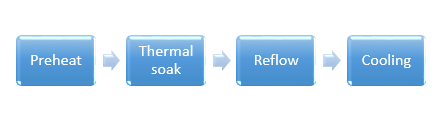
In the preheat stage, heat is accumulated in the board and the components. The temperature should gradually change because quick changes in temperature can damage the components. Generally, the temperature change is no more than 2°C/second. This information can be found in the solder paste datasheet.
During the thermal soak stage, the oxidation of pads and leads of components are reduced by activating the flux.
In the reflow stage, the solder paste is melted and the process reaches its maximum temperature (lesser than the maximum allowed temperature of the components). The processed board is then cooled down and the solder alloy solidifies to create solder joints.
In the further stages, the flex board is optically inspected and electrically tested to ensure it is 100% error free. Post testing, it is punched out of the panel and sent to final quality check (FQC). After FQC the circuit board is sent to packaging and warehousing.
Sierra Circuits engineers and technicians have the experience to bring your flexible circuits to life.
Start a custom quote now.
Design considerations for flex PCB assembly
Important flex PCB assembly specifications that a designer needs to know.
- Base materials: The most common base material used in flex boards is polyimide films. These materials are flexible and thin. Choose a material with good thermal resistance and electrical conductivity.
- Number of layers: The number of layers in a flexible PCB depends on the type of application it is used in. For dynamic applications, opt a single layer board. For static, the number of layers can vary from 4 to 8.
- Bend radius: The bend radius of a flex circuit determines the bendability of it. Generally, the bend radius of these boards vary between 1 mm and 5 mm.
Flex PCB Design Guide
10 Chapters - 39 Pages - 45 Minute ReadWhat's Inside:
- Calculating the bend radius
- Annular ring and via specifications
- Build your flex stack-up
- Controlled impedance for flex
- The fab and drawing requirements
Download Now
Characteristics of flex board assembly
Application of auxiliary fixtures
Flex boards are prone to wear and tear as they are thin and light weighted. To successfully assemble SMT components, rigid carriers are used. The positioning and consistency of the carrier plays a vital role in the assembly process. Lots of auxiliary fixtures are implemented in flex assembly, including board carrying tray, baking, electrical test, function test, and cutting fixtures.
Low density
The number of components that can be assembled on flex PCBs is relatively low when compared to rigid boards.
High quality requirements
Generally, these boards are used in places where it requires repeated flexing. The components assembled have to meet the demands of their operating conditions. Therefore, flex circuit boards demand higher standards in terms of cleanliness and soldering reliability than rigid PCBs.
High assembly cost
Compared to rigid PCB assembly, flex assembly expenses are higher with longer manufacturing duration. The process demands more accessories and staff, and requires a well maintained manufacturing environment.
To learn more about flex design guidelines, download our Flex PCB Design Guide.


