PCB Design for Assembly Handbook
Our DFA Handbook outlines a reliable system to help you reduce cost and speed up the assembly of your prototypes.


Sierra Circuits’ Design for Assembly Handbook shows you how to prepare your PCB layout for reliable assembly. It covers key design practices such as component selection and placement, spacing, documentation, testing, and quality control.
Here’s a quick breakdown of what you’ll learn in this handbook:
- Why design for assembly (DFA) matters for reducing assembly costs and production issues
- How component selection and availability affect assembly
- Key considerations for part placement, spacing, and clearance
- How to prepare designs for automated assembly and testing
- Which file formats and documentation are required for assembly
- Best practices for silkscreen, thermal relief, and board layout
- What testing methods can be used before and after assembly
- Common assembly defects, their causes, and prevention methods
- Quality control, inspection, and IPC requirements for production
- Assembly tolerances and clearance requirements
- Factors that affect assembly costs
The following sections will provide you with a closer look at each of these topics:
Why is design for assembly important?
Following DFA rules helps you to reduce PCB assembly costs, prevent production issues, and make the transition from prototype to production more efficient.
Design for assembly focuses on reducing unnecessary components, making parts easier to assemble, and considering assembly requirements while the design is still being developed.
DFA considerations can vary between prototype and production boards. Prototypes focus on circuit and functional validation, while production designs place greater emphasis on testability and manufacturing needs.
Regardless of production stage, key objectives include verifying component availability, matching manufacturing part numbers with footprints, checking component placement and spacing, and confirming solder mask, solder paste, and DNI markings.
The handbook also covers practical assembly considerations, including manufacturer-recommended footprints, component and drill clearances, thermal relief, trace routing, board edges, and the operating environment.
How to improve your assembly yield through better design?
Reducing component count, using standard parts, simplifying fastening, and designing for automation and testing can make assembly more efficient.
The handbook covers PCB handling, soldering methods, footprint design, error prevention, and assembly documentation as key parts of the DFA process.
Designs intended for automation should use consistent components, suitable tolerances, self-aligning features, and orientations. Test planning should account for bare-board and post-assembly testing, including isolation, continuity, shorts, in-circuit testing, and flying probe testing.

Assembly notes should provide the manufacturer with necessary information, including board class, layer count, thickness, IPC standards, solder mask and silkscreen details, impedance, cut-outs, stack-up, drill information, and revision details.
How to build assembly-friendly circuit board designs?
Key DFA considerations include PCB design data, component placement, clearances, thermal relief, quality control, inspection, and applicable IPC standards. Addressing these requirements helps manufacturers interpret the design correctly, source components, assemble the board consistently, and catch problems early.
Prepare complete manufacturing data
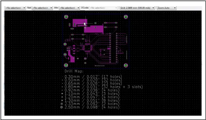
A comprehensive manufacturing package should include Gerber/ODB++/IPC-2581, IPC netlist, drill files, BOM, pick-and-place files, and fabrication drawings. Gerber provides layer-specific design data, while ODB++ can combine placement, BOM, material construction, dimensions, and fabrication information into a single data structure.
Follow layout and placement guidelines
Use readable silkscreen, adequate component spacing, proper part-to-edge and part-to-hole clearances, and sufficient courtyard space for inspection and rework. Component placement should also account for sensitive components, board warpage, inspection access, and depanelization.
Check component availability
Verify component availability throughout the design process. Where possible, identify alternate parts early to avoid sourcing issues and production delays later.
Design for reliable thermal relief
Thermal relief is important when pads connect to large metal areas. Spoke width and count should provide the required power conduction while still supporting reliable soldering. Also check closely spaced pads and small or split metal areas to ensure proper connectivity.
Plan for inspection and testing
Final inspection and testing are easier when the workspace and equipment are organized for accessibility. The process should provide clear inspection points and the right equipment to identify assembly defects before the board reaches the customer.
Follow applicable IPC standards
Relevant standards include IPC-A-600 for circuit board acceptability and IPC-A-610 for electronic assembly acceptability. IPC-A-610 defines three assembly classes, ranging from Class 1 for general-purpose products to Class 3 for products requiring higher levels of reliability.
Addressing these DFA requirements early can help you reduce PCB assembly defects, rework, delays, and unexpected production costs.
What are the typical design issues that lead to assembly defects?
Footprint mismatches, missing orientation or polarity markings, incomplete component data, unavailable parts, missing CAD layers, and inconsistencies between BOM, CAD, and placement files can cause assembly problems. Resolving these issues before assembly helps prevent delays and ensures components can be correctly identified, sourced, and placed.
A footprint mismatch occurs when the component listed in the BOM does not match the footprint in the CAD data, which can prevent the component from being assembled correctly. Missing or incorrect mounting orientation, pin 1, cathode, or positive-terminal markings can also make component placement unclear. When a component datasheet is unavailable, mechanical or package dimensions may be needed for DFA validation.
The handbook also identifies component overlap, missing BOM components in Gerber or placement files, unavailable stock, missing paste or mask layers, and missing pads as common issues. When parts are unavailable in the required quantity, possible solutions include using an alternate manufacturer part, customer-supplied components, or marking the component as DNI (Do Not Install).
Other issues include missing reference designators, incorrect polarity markings, unresolved alternate parts, incomplete part information, quantity mismatches, and VPN-to-MPN inconsistencies. Updated silkscreen, XY, CAD, or other revised files may be required before production can proceed.
Open solder joints, solder bridges, and component shifts are common assembly defects that can impact PCB quality. Understanding their causes can help you and production engineers prevent defects and improve assembly quality and yield.
Open solder joints occur when a component lead does not form a proper connection with its pad. Insufficient or inconsistent solder paste, gaps between the lead and pad, contamination, inactive solder paste, and an unsuitable reflow profile can contribute to the defect. Proper stencil design, accurate component placement, material handling, and controlled reflow can help prevent it.
Solder bridges, or shorts, occur when solder connects adjacent leads or pads that should remain electrically separate. Excess solder, unsuitable pad geometry, stencil issues, poor alignment, and incorrect component placement can contribute to bridging. Proper paste deposition, stencil alignment, and reflow control can help reduce the risk.
Component shift occurs when a component moves from its intended position, often during reflow. Part-to-pad geometry, bent leads, uneven heat distribution, vibration, poor solder deposition, excessive convection, and unsuitable heating rates can contribute to the problem. Proper placement and clearance, accurate placement equipment, careful handling, and controlled solder deposition can help minimize component shift.
What tolerances and clearances matter for PCBAs?
Component tolerances, part spacing, hole and board-edge clearances, stencil alignment, and panel dimensions are important DFA considerations that affect how reliably a PCB can be assembled.
Component tolerances and storage
Part values can vary from their nominal ratings, so these tolerances should be considered during circuit design. The handbook also highlights storage requirements for moisture-sensitive components. For example, BGA devices should be stored at 20 to 25°C and 10% RH and assembled within 8 hours after removal from storage. In addition, baking at 125°C can remove absorbed moisture before soldering.
Part clearances
Component spacing directly affects soldering quality. Insufficient clearance can lead to tombstoning, misalignment, solder bridging, and inadequate solder. The handbook recommends 0.15 mm (6 mil) clearance for components smaller than 0603, 1 mm (39 mil) for sensitive devices such as BGAs, and 0.5 mm for connectors, crystals, and canned capacitors. It also provides minimum spacing values for different passive component packages.
Hole and board-edge clearances
Clearance around holes, annular rings, and board edges also requires attention. The minimum component-to-hole-wall spacing is 8 mils, while manual soldering may require 50 to 100 mils. Component-to-annular-ring spacing should be at least 7 mils, with 50 to 100 mils recommended for manual soldering. Board-edge clearance varies by component size, with 125 mils for larger components, 25 mils for smaller components, and 10 mils for manually installed parts.
Stencil alignment and fiducials
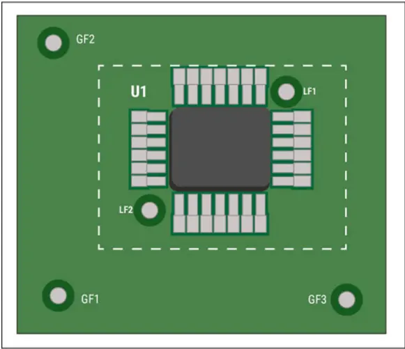
Accurate stencil alignment depends on properly placed fiducial markers. The handbook recommends circular, non-drilled copper marks without solder mask, typically 1 to 3 mm in diameter, with 3 mm clearance from the board edge. Three global fiducials(GF) can establish board orientation, while two local fiducials (LF) can help identify the footprint of a quad-packaged SMT component.
Panel dimensions
Panel dimensions affect board handling during production. The handbook lists standard panel sizes of 24 × 18 inches, 12 × 18 inches, 24 × 9 inches, and 12 × 9 inches, with 0.1 inch spacing between individual boards. Minimum clearance requirements are 1 inch for single-sided boards and 0.5 inch for double-sided boards.
What are the cost drivers of your PCBA?
Turnaround time, assembly technology, component packages, production volume, component count, and board construction can drive assembly costs. Evaluating these factors early can help you make the right decisions before production begins.
Expedited (fast-track) production can increase costs by 30% to 200% compared with conventional turnaround time, as the manufacturer may need to prioritize the order or adjust production resources.
Surface-mount technology is generally more cost-effective than through-hole technology (THT) because of lower setup costs, higher component density, and greater automation. THT can increase costs when additional drilling and reduced routing area are involved.
Component packaging affects inspection and placement costs. BGA and QFN packages require greater placement accuracy because their connections are underneath the component and may require X-ray inspection for voids and shorts. Conventional packages such as SMD, 0603, 0805, and 1206 do not carry the same assembly costs.
Production volume and component count also affect the final price. Higher-volume production can reduce one-time setup costs through economies of scale. Prototype runs may require separate setup costs. More components increase assembly cost directly.
Following DFA guidelines helps you reduce potential PCB assembly errors and improve overall assembly yield. Download the Design for Assembly Handbook to learn more.