Flex PCB Specs


The Pitch

Get low-to-high volume flex, rigid-flex and HDI Flex PCBs manufactured with industry leading quick turnaround times.

  • Freedom of design
  • Reduced space and weight
  • Increased reliability and durability.
  • Improved heat dissipation and airflow
  • Use in harsh environment

The Parameters

  • Three types of flex designs: flex, rigid-flex and HDI flex
  • Special stack-up help / NPI review
  • Up to 12 layers for flex and 16 layers for rigid-flex
  • The most effective PCB layout for compact devices
  • Quote sent by email within a few hours
Start an Online Quote
LEARN PCB
PCB Manufacturing
PCB Assembly
PCB Design and Layout
PCB Basics
Vias, Drilling & Throughplating
Mechanics
Surface
SMD
Quality
SPECIFICATIONS
PCB Fabrication
STANDARDS & POLICY
PCB Ordering
Policy
PCB Attributes
Min Layer Count 1 1
Max Layer Count 12 ≥ 16
Min Core thickness .001″ (.025 mm) .002″ (.051 mm)
Max Finished Copper Weight (I/L) 2 oz (59 ml) 3 oz (89 ml)
Max Finished Copper thickness (O/L) 12 micron (.012 mm) 9 micron (.009 mm) (only for O/L)
Max Panel Size 12×18 12×18
Smallest Mechanical Drill Diameter .0079″ (.201 mm) .0071″ (.180 mm)
Smallest Laser Drill Diameter No .005″ (.127 mm)
Min Finished Hole Size .006″ (.152 mm) .006″ (.152 mm)
Max through Hole Aspect Ratio 10:1 10:1
Max Blind Via Aspect Ratio .75:1 .75:1
Min Trace and Space ≤ .0035″ (.089 mm) ≤ .0030″ (.076 mm) (rigid)
Min Pad Size for Test .016″ (.406 mm) .005” (.127 mm) (rigid)
Process Pad Diameter D + .014″ (.356 mm) (1-mil (.025 mm) annular ring) D + .014″ (.356 mm) (1-mil (.025 mm) annular ring)
Stacked Vias No No
Min Wire Bond Pad Size > .006″ (.152 mm) > .006″ (.152 mm)
Controlled Impedance Tolerance 10% 5%
Solder Mask Registration Within .002″ (.051 mm) Within .002″ (.051 mm)
Solder Mask Feature Tolerance .001″ (.025 mm) .001″ (.025 mm)
Solder Mask Min Dam Size .004″ (.102 mm) .001″ (.025 mm)
Min Diameter Route Cutter Available .019″ (.483 mm) .024″ (.610 mm)
Mechanical Routed Part Size Tolerance .003″ (.076 mm) .010″ (.254 mm)
Bow and Twist Tolerance N/A As per spec
Thickness Tolerance +/- .002″ (.051 mm) 10%
Sequential Laminations n/a 2
Buried Vias Yes Yes
Blind Vias Yes Yes
Conductive Filled Vias No Yes
Non Conductive Filled Vias No Yes
Surface Finishes
HASL (Vertical or Horizontal) Yes (not recommended) Yes
Lead Free HASL Yes (not recommended) Yes
OSP (Shikoku F2) Yes (not recommended) Yes
OSP (Entek) Yes (not recommended) Yes
ENIG (Electroless Nickel/Immersion Gold) Yes (most common) Yes
Immersion Silver Yes (not recommended) Yes
Immersion White Tin No No
Tin Nickel No No
Electrolytic Soft Gold Yes Yes
Electrolytic Hard Gold Yes Yes
Selective Gold Yes Yes
Solder Mask Colors
Amber Yes Yes
Green Yes Yes
Black No Yes
Red No Yes
Blue No Yes
Yellow No Yes
White No Yes
Clear No Yes
Bright White No Yes
Purple No Yes
Legend
White Yes Yes
Fab
Routed Array Yes Yes
V Score, Edge to Copper .002″ (.051 mm) .01″ (.254 mm)
V Score Angles No Yes
Countersink Yes Yes
Counterbore Yes Yes
Bevel Yes Yes
Milling Yes Yes
Edge Castellation Yes Yes
Edge Plating Yes Yes
Heatsinks No No
Electrical Test
10 Volt Yes Yes
40 Volt (Burn-In Boards) Yes Yes
250 Volt Yes Yes
500 Volt Yes Yes
Flexible Poyimide Yes Yes
Arlon 85NT No No
Bergquist No No
Hybrid Constructions Yes Yes
Isola FR406 Yes Yes
Isola FR408 HR Yes Yes
Isola P95 Yes Yes
Isola P96 Yes Yes
Iteq IT180 Yes Yes
Panasonic R1766 Yes Yes
Panasonic R1755 Yes Yes
Panasonic Megtron Yes Yes
Nelco N4000-13 Yes Yes
Nelco N4000-29 Yes Yes
Nelco BT N5000 Yes Yes
Nelco N7000-2 Yes Yes
No Flow Prepreg Yes Yes
Isola 370HR v Yes
Polyclad Getek No No
PSA Bond Film Yes Yes
Rogers 3000 Series No No
Rogers R4000 Series No No
Rogers 5000 Series No No
Rogers 6000 Series No No
Rogers TMM No No
Available Reports
Microsection Yes Yes
Solderability Yes Yes
X-Ray Fluorescence Yes Yes
Ionic Contamination Yes Yes
Time Domain Reflectometry Test (TDR) Yes Yes
FAI Yes Yes
Certificate of Compliance Yes Yes
UL
94VO Yes Yes
PCB Classifications Mil-Spec
MIL-PRF-55110 No No
MIL-PRF-31032/1 No No
MIL-PRF-31032/2 No No
IPC 6012, Class 1, 2 and 3 Yes Yes
ISO 9001:2015 Yes Yes
ISO 13485:2016 Yes Yes
LEARN PCB
PCB Manufacturing
PCB Assembly
PCB Design and Layout
PCB Basics
Vias, Drilling & Throughplating
Mechanics
Surface
SMD
Quality
SPECIFICATIONS
PCB Fabrication
STANDARDS & POLICY
PCB Ordering
Policy

Sierra Circuits is
headquartered in Silicon Valley.
We welcome visitors at
our 70,000 sqft facility,
located at 1108 West Evelyn Avenue
in Sunnyvale, California.
Book a tour with an account manager today!
Let us introduce you to one of the most innovative communities of engineers and designers in the world.
We can help you plan your project from design to assembled board.

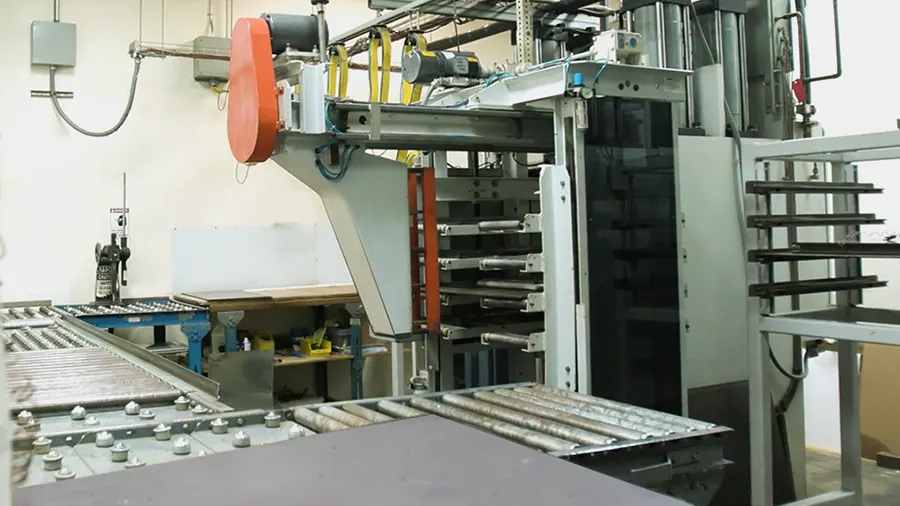
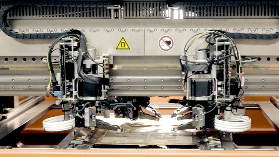
Manufacturing Equipment at Sierra Circuits

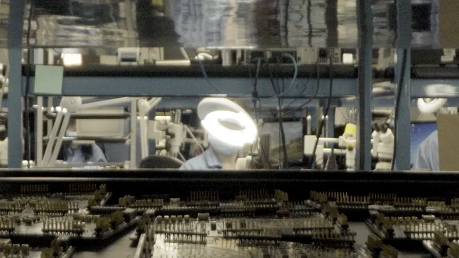
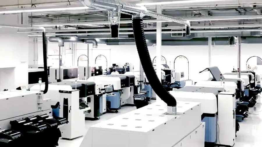
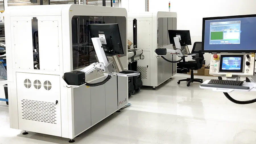
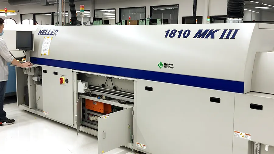
Our 70,000 sqft state-of-the-art campus in the heart of Silicon Valley contains the most advanced equipment required for the manufacture and assembly of your PCBs. Whether you’re looking for standard quick turn PCBs or boards with the tightest tolerances, made from exotic metals, there’s a reason Sierra Circuits leads the industry in quality and performance.

PCBs manufactured and assembled in the United States

Turn-times as fast as 1 day.

Sierra Circuits can manufacture your PCB and have it expedited to you within 24 hours.

Full turnkey boards, with assembly and components in as fast as 5 days.

Get an Instant, Itemized Quote

Talk to a Sierra Circuits PCB Expert today

24 hours a day, 7 days a week.

Call us: +1 (800) 763-7503
Book a Meeting with a Sales Rep
Email us: through our Customer Care form