Surface-mount devices are mounted directly to a PCB. These components are smaller than the through-hole components and comprise a small lead or no lead at all. Since SMD components require fewer drilled holes, they incorporate higher routing density, and the design becomes more compact.
There are many SMD components of different package sizes with various functionalities. They can be placed on both sides of the circuit board, along with a higher component density, with more connections possible per component to attain higher speed. Here, we will briefly introduce some of them.
SMD package sizes for resistors, capacitors, inductors, and diodes
SMD passive components consist of resistors, capacitors, and inductors with a rectangular package. Diodes are also part of this, but are two-terminal active devices. Diodes can be miniaturized and packaged according to the following SMD sizes.
| Chip package type | Dimensions in mm | Dimensions in inches |
|---|---|---|
| 01005 | 0.4 x 0.2 | 0.016 x 0.008 |
| 015015 | 0.38 x 0.38 | 0.014 x 0.014 |
| 0201 | 0.6 x 0.3 | 0.02 x 0.01 |
| 0202 | 0.5 x 0.5 | 0.019 x 0.019 |
| 02404 | 0.6 x1.0 | 0.02 x 0.03 |
| 0303 | 0.8 x 0.8 | 0.03 x 0.03 |
| 0402 | 1.0 x 0.5 | 0.04 x 0.02 |
| 0603 | 1.5 x 0.8 | 0.06 x 0.03 |
| 0805 | 2.0 x 1.3 | 0.08 x 0.05 |
| 1008 | 2.5 x 2.0 | 0.10 x 0.08 |
| 1111 | 2.8 x 2.8 | 0.11 x 0.11 |
| 1206 | 3.0 x 1.5 | 0.12 x 0.06 |
| 1210 | 3.2 x 2.5 | 0.125 x 0.10 |
| 1806 | 4.5 x 1.6 | 0.18 x 0.06 |
| 1808 | 4.5 x 2.0 | 0.18 x 0.07 |
| 1812 | 4.6 x 3.0 | 0.18 x 0.125 |
| 1825 | 4.5 x 6.4 | 0.18 x 0.25 |
| 2010 | 5.0 x 2.5 | 0.20 x 0.10 |
| 2512 | 6.3 x 3.2 | 0.25 x 0.125 |
| 2725 | 6.9 x 6.3 | 0.27 x 0.25 |
| 2920 | 7.4 x 5.1 | 0.29 x 0.20 |
Comparison of different SMD components
It’s crucial to select the right SMD components that not only fit into your design but also fulfill its intended purpose effectively. The table below provides a comparison among commonly used SMD components:
| Packages | Dimensions (mm) | Applications | Component type | Number of pins |
|---|---|---|---|---|
| SMA | 3.56 x 2.92 | RF and microwave devices | Diode | 2 |
| DO-214 | 5.30 x 6.10 | Power rectification diodes | Diode | 2 |
| DO-213AA | 4.57 x 3.94 | Small signal transistors and diodes | Diode | 2 |
| SMC | 5.94 x 5.41 | Integrated circuits, resistors, and capacitors | Diode | 2 |
| TO-277 | 3.85 x 3.85 | Power MOSFETs and voltage regulators | MOSFET | 3 |
| MBS | 2.60 x 1.90 | Switching diodes and high-density integrated circuits | Diode | 2 |
| SOD-123 | 2.60 x 1.90 | Small signal diodes and transistors | Diode | 2 |
| 0603 | 1.6 × 0.8 | Consumer, automotive, and industrial equipment | Resistors, capacitors, and inductors | 2 |
| 0805 | 2.0 × 1.25 | Consumer, automotive, and industrial equipment | Resistors, capacitors, and inductors | 2 |
| 1206 | 3.2 × 1.6 | Consumer, automotive, and industrial equipment | Resistors, capacitors, and inductors | 2 |
Surface-mount PCB connectors
An electronic project is incomplete without a proper connector. In surface-mount technology, SMA and SMB connectors are mostly used for board assembly. SMA and SMB stand for sub-miniature version A and sub-miniature version B.
| Type | Properties | Application |
|---|---|---|
| SMA | 1. Semi-precision 2. Coaxial RF connector 3. Impedance 50Ω 4. Electrical use from DC (0 GHz) to 12 GHz, but extended to 18 GHz and 26.5 GHz | 1. Microwave systems 2. Hand-held radio 3. Mobile telephone antennas 4. WiFi antenna systems |
| SMB | 1. Semi-precision 2. Coaxial RF connector 3. Impedance 50Ω or 75Ω 4. Electrical use from DC(0 GHz) to 4 GHz 5. Smaller than SMA | 1.Telecommunications 2. Test equipment 3. Instrumentation 4. GPS |
Connector Design Guide
5 Chapters - 32 Pages - 50 Minute ReadWhat's Inside:
- Basics
- Terminology
- Selection and layout rules
- Testing
- Application-specific PCB connectors
Download Now
Common SMD Tantalum capacitor sizes
Tantalum capacitors do have very high capacitance with very small packaging. These capacitors give the best results in high-capacitance, low-current environments.
| Package type | Dimensions in mm | EIA standard |
|---|---|---|
| Size A | 3.2 x 1.6 x 1.6 | EIA 3216-18 |
| Size B | 3.5 x 2.8 x 1.9 | EIA 3528-21 |
| Size C | 6.0 x 3.2 x 2.2 | EIA 6032-28 |
| Size D | 7.3 x 4.3 x 2.4 | EIA 7343-31 |
| Size E | 7.3 x 4.3 x 4.1 | EIA 7343-43 |
Small outline transistor package types
A small outline transistor is a discrete surface-mount transistor that is mainly used in consumer electronics. Here are some commonly used SOTs.
| Package type | Dimensions in mm | Terminal |
|---|---|---|
| SOT-23 | 3 × 1.75 × 1.3 | 3 |
| SOT-223 | 6.7 × 3.7 × 1.8 | 4 |
| SOT-323 | 2.1 x 2.1 x 0.9 | 4 |
| SOT-523 | 1.6 x 1.6 x 0.7 | 4 |
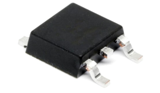
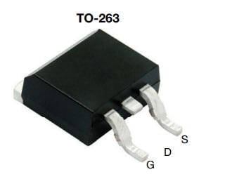
Other SMD transistors
We can see some popular SMD transistors other than SOT here.
TO-252-3 (DPAK)
TO-263
Integrated circuit SMD packages
ICs are enclosed in a package for protection. Here, we will see some important IC packages, their properties, and applications.
| Package type | Properties | Application |
|---|---|---|
| SOIC | 1. Small outline integrated circuit 2. Surface-mount equivalent of the classic through-hole DIP (Dual-Inline Package) | 1. Standard package for logic IC |
| TSSOP | 1. Thin shrink small outline package 2. Rectangular surface mount 3. Plastic integrated circuit (IC) package 4. Gull-wing leads | 1. Analog amplifiers, 2. Controllers and Drivers 3. Logic devices 4. Memory devices 5. RF/Wireless 6. Disk drives |
| QFP | 1. Quad flat package. 2. Easiest option for high pin-count components 3. Easy to inspect by AOI 4. Assembled with standard reflow soldering | 1. Microcontrollers 2. Multi-channel codecs |
| QFN | 1. Quad flat no-lead 2. Electrical contacts do not come out of the component 3. Smaller than QFP 4. Require extra attention in PCB assembly | 1. Microcontrollers. 2. Multi-channel codecs |
| PLCC | 1. Plastic leaded chip carrier 2. Allow components to be directly mounted on the PCB | 1. Prototype PCB assembly |
| BGA | 1. Ball grid array 2. Most complex 3. High-pin count component 4. Electrical components are below silicon IC 5. Requires reflow soldering for PCB assembly | 1. High-speed microprocessor 2. Field programming gate array(FPGA) |
| POP | 1. Package-on package technology 2. Stacked on the top of others | 1. Used for memory devices and microprocessors. 2. High-speed design, HDI design |
SMD components ensure a smaller form factor design. The manufacturing cost is minimized, and board space can be efficiently optimized by incorporating these components. Indeed, SMD packages are the better choice over through-hole components when designing a sleek, compact, high-speed, or HDI board.


