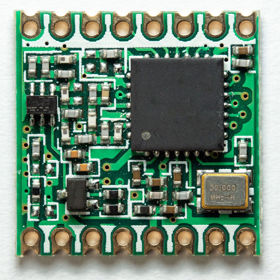
What are castellated holes/plated half-holes?
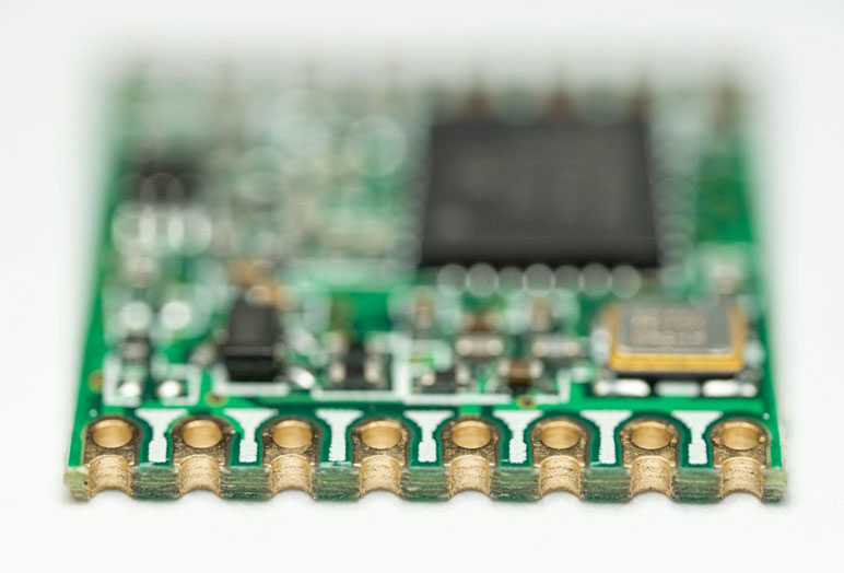
Castellated holes are preferred when a PCB module, like a Wi-Fi or Bluetooth module, needs to be mounted on another circuit board. They resemble the plated through-holes, but they are half the shape of a hole, hence the name. So basically, castellated holes are PTHs with their center at the board outline. Their purpose is to allow individual board modules to be soldered easily onto other circuit boards.
Also, see plated-through slots to properly accommodate rectangular leads and improve mechanical and electrical reliability.
Why are plated half-holes required?
As mentioned earlier, the primary intention is to connect the castellated circuit board to different modules. When a module is soldered to another PCB, that process is called board-to-board soldering. Below are the reasons why castellated holes are required in board-to-board soldering.
- Easy access and soldering:
Since they are half-holes and placed on the side of the module, accessing them is very easy. Having SMD pads at the bottom of a module will create an obstacle for component placement. Hence, plated half-holes are provided. Since they are present on the edge, soldering becomes easy. - Proper alignment:
When the pads are under a module, they can lead to misalignments. But when the holes are on the side of the PCB, the chances of alignment errors are reduced. - Easy measurements:
When the plated half-holes are used, measurements of distances between the holes and the solder become easier. We can measure the distance using calipers even after the placement of the module. This is not possible if the pads for soldering are beneath the module. - Cleaner board surfaces:
The PCB modules that have castellated holes are considered surface-mount sub-assemblies. Hence, they will fit directly onto another circuit board just like an SMD component. Therefore, the chances of dust and dirt getting accumulated between the two boards are negligible as the connection is pretty tight.

Design for Manufacturing Handbook
11 Chapters - 96 Pages - 90 Minute ReadWhat's Inside:
- Annular rings: avoid drill breakouts
- Vias: optimize your design
- Trace width and space: follow the best practices
- Solder mask and silkscreen: get the must-knows
Download Now
How are castellated holes designed?
Designing plated half-holes is similar to designing through-holes. In the PCB design, these holes are kept with their centers on the designated board outline. Thus, half of the plated hole will be on the board, and the other half will be outside.
If you are designing castellated modules, keep all the components of the module on the top side. Similarly, the circuit board to which the module needs to be mounted should not have any components on that entire portion.
How are the castellated holes manufactured?
Once these holes are designed, manufacturing takes place through a unique process. As a designer, you need to convey your requirements to the fabricator prior to the manufacturing process. For adding these features, regular milling tools cannot be used. The tools can get damaged while milling since these half-holes are plated with copper. Therefore, this requires heavy-duty milling bits. Once the milling process is completed, the holes are cleaned up, inspected, and deburred.
Castellated holes assist easy installation of modules and also ease the inspection of connections.


