What is E-test in a PCB?
E-test is the electrical test done on a bare printed circuit board. It is the final step in the PCB manufacturing process. Here, electrical probes are used to check for shorts, opens, resistance, capacitance, and other fundamental electrical properties on unpopulated boards. This test is crucial to determine the quality of the board.
PCB E-test examines the electrical conductivity of the circuit board with respect to the netlist file obtained from the schematic. The netlist provides information on a board’s conductivity interconnection patterns. E-tests can be carried out using two methods:
- Flying probe
- Fixture method
The criteria for choosing these methods vary as per requirements.
E-test method 1: FPT
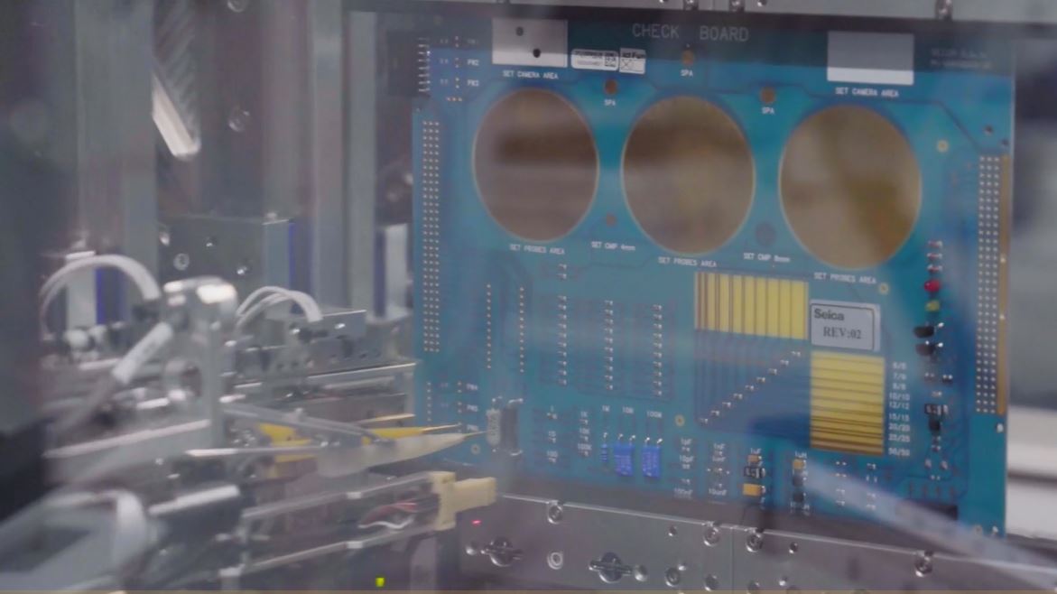
Flying probe testing uses probes that move from one test point to another according to the instructions provided by a specific software program. This is a fixtureless test method.
FPT checks shorts and opens on a bare board. On a populated board, it verifies the capacitance, inductance, resistance, and component values.
A flying probe test program (FTP) is created using Gerber, ODB++, or IPC-2581.
Once the program is generated, it is loaded into the FTP tester. According to the test program, the tester will apply electrical signals and powers to the probe points and records the measurement.
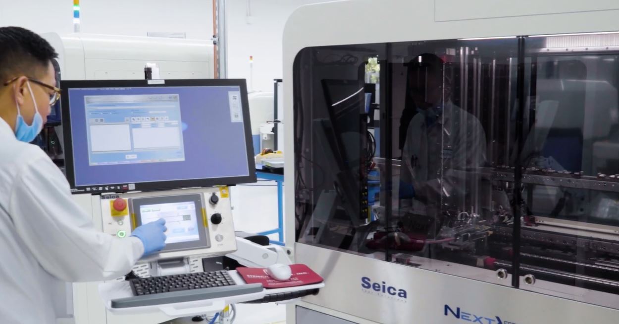
We implement Seica Spa Pilot V8 for flying probe testing. This hi-tech, latest machine provides maximum performance, increased test speed, and low to medium volume run.
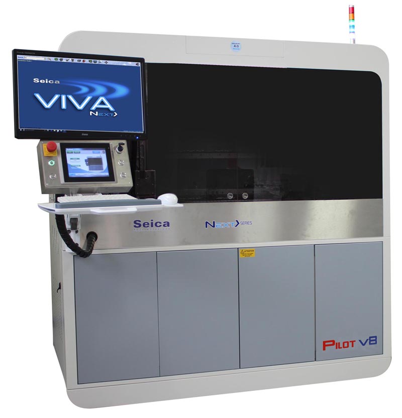
The simultaneous vertical probing feature of this tester quickens the debugging process and enhances the flexibility for prototyping.
Design for Testing Handbook
7 Chapters - 28 Pages - 45 Minute ReadWhat's Inside:
- PCB testing strategies
- Guidelines to design and place a test point for FPT
- Directives to make your board ICT compatible
- Benefits and drawbacks of various testing methods
- Defects that you can identify through board testing
Download Now
Advantages of a flying probe tester
- Flying probes do not need fixtures and FPT programs can be easily generated.
- It is a cost-effective method for small-volume production.
- Flexible testing approaches can be implemented using specific software programs.
E-test method 2: Fixture method
The fixture method, popularly known as a bed of nails testing, is a conventional PCB electrical testing method. This method requires the creation of a test template with pins aligned to the test locations in the circuitry.
The templates are formed by inserting pogo pins into holes on an epoxy phenolic glass-cloth-laminated sheet. Stable connections will be verified immediately when a bare board is pressed down against the fixture. These connections will have hundreds of test points within the circuitry of the PCB. The fixture method is time-consuming and requires a high material cost as well as specialized jigs to create the initial fixture. Though the bed of nails testing is a time-consuming process, it allows rapid testing after the fixture is created. This process is fast and suitable for mass production systems.
The E-test methods (flying probe test and bed of nails) have their own benefits and limitations in terms of efficiency, time, and cost. It is better to decide based on the requirements of the circuit board. Electrical testing for PCBs is essential to verify the functionality of a PCB.


