What is ENIG in PCB surface finishes?
Electroless nickel immersion gold (ENIG ) is a two-layer metallic surface finish that consists of a very thin layer of gold plated over a layer of nickel. Using an electroless chemical reaction, a nickel layer is first plated on copper pads. An immersion method is then used to apply gold on top of the nickel layer to cover the pads and traces.
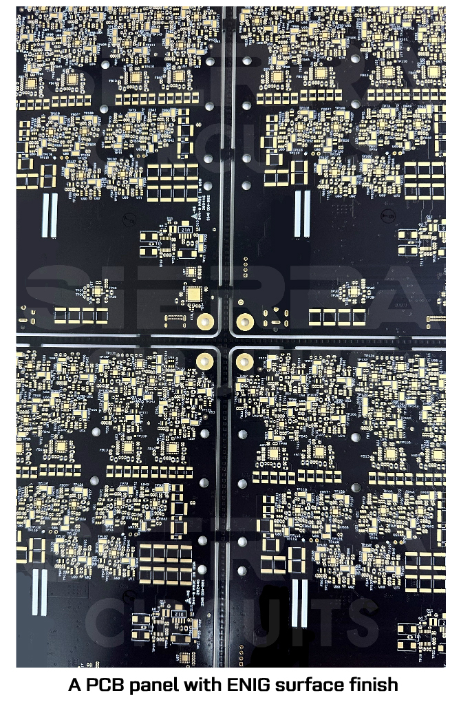
The gold layer protects the nickel during shipping, resulting in a longer shelf life. This finish also creates a flat surface that is suitable for mounting parts like SMDs and ball grid arrays (BGAs). ENIG is preferred by many PCB assemblers due to gold’s high electrical conductivity. This surface finish is RoHS (restriction of hazardous substances) compliant.
Here’s a quick overview of ENIG PCB surface finish:
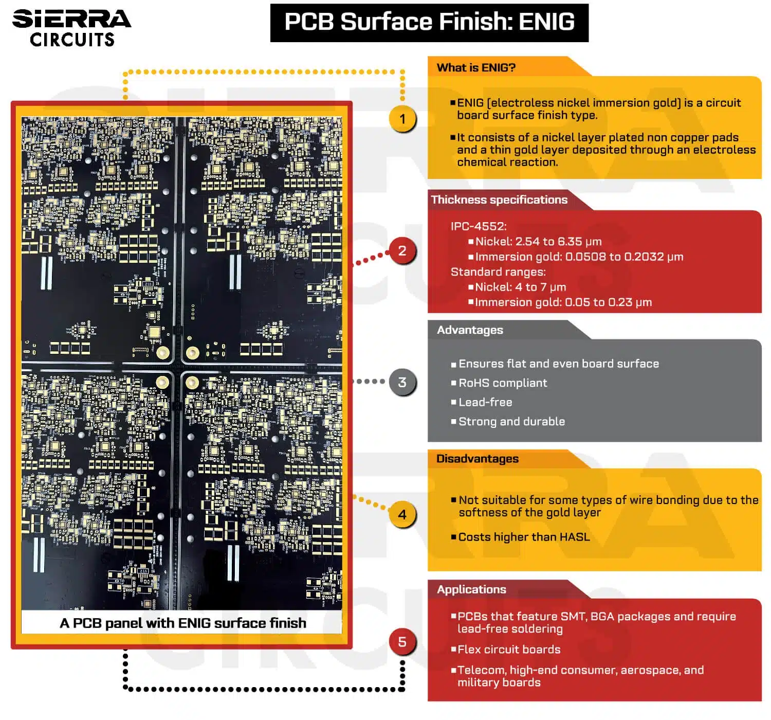
Also, see types of circuit board surface finishes.
Thickness specifications
ENIG is a metallic coating in which nickel acts as a barrier to the copper pad. Gold, on the other hand, protects the nickel during the storage period and has a low contact resistance. Nickel thickness ranges from 4 to 7 µm, while gold thickness ranges from 0.05 to 0.23 µm. This finish requires a temperature of about 80°C for processing.
We use IPC specifications unless the customer has a special request. The coating thickness can be checked by the XRF (X-ray fluorescence spectroscopy) technique.
| IPC-4552 thickness specifications for ENIG | |
|---|---|
| Nickel | 2.54 to 6.35 µm (100 to 250 µin) |
| Immersion Gold | 0.0508 to 0.2032 µm (2 to 8 µin) |
IPC Class 3 Design Guide
8 Chapters - 23 Pages - 35 Minute ReadWhat's Inside:
- IPC guidelines for manufacturing defects
- IPC standards for assembly processes
- Common differences between the classes
- IPC documents to set the level of acceptance criteria
Download Now
Black pad defect
The ENIG process is responsible for the formation of black pads. Although the process provides a highly solderable finish, which is ideal for applications where durability and complex circuitry go hand in hand, it can also result in defective joints that will break their connections when stressed. The resulting open circuits expose a corroded layer of dark nickel, popularly known as a black pad. It is the result of excessive phosphorus that is formed as a byproduct of the dissolution of nickel. However, there are a few workarounds to avoid black pads.
When gold is plated during the ENIG process, it depends on a corrosion reaction to place itself (gold) on top of the nickel substrate. Aggressive gold baths and high gold thickness can increase corrosion, which leads to a black pad.
It is similar to brittle fracture because it creates a cracked structure within the nickel after the gold has been plated and then removed. Vibrations, thermal stress, and shocks can then weaken the metallurgical bonds.
Since ENIG finishes cannot be reworked, the best way to avoid a black pad problem is its prevention. This is done by maintaining strict control over the nickel bath, where the gold-to-nickel exchange is held as close to ideal as possible. One of the most important aspects is to carefully observe the pH level in the nickel bath, as this will indicate the level of phosphorus present.
EPIG surface finish is one of the newer technologies, introduced as an alternative to electroless nickel immersion gold (ENIG). Unlike ENIG, it eliminates the use of nickel, avoiding nickel-related black pad corrosion issues.
For a cost-effective, ultra-flat surface finish ideal for nickel-sensitive applications, see OSP surface finish.
Pros and cons of ENIG
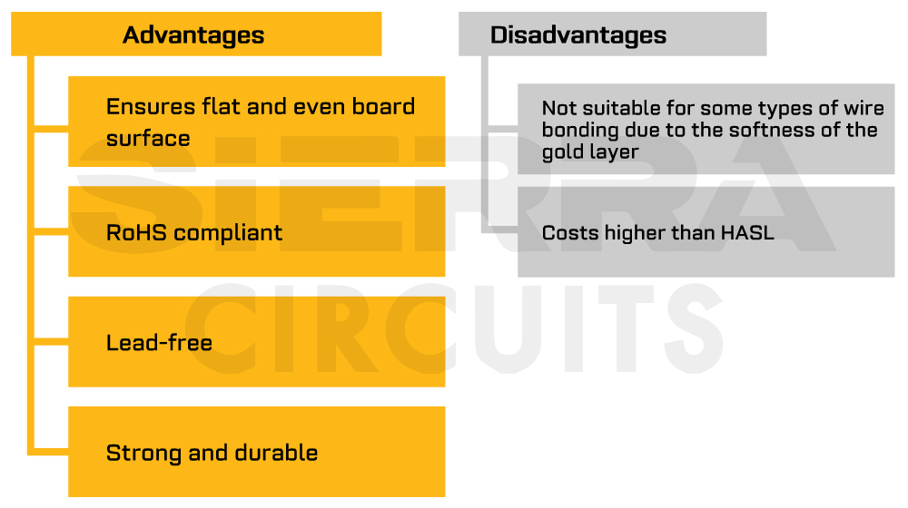
The advantages and disadvantages of electroless nickel immersion gold are listed in the chart below:
If your application involves edge connectors or repeated insertion cycles, read our knowledge base, gold fingers, which are specifically designed to handle mechanical wear and ensure reliable contact performance.
Applications of ENIG
ENIG is mainly used in SMT, lead-free soldering, and BGA packages. ENIG serves industries such as data/telecom, high-end consumer, aerospace, military, and high-performance devices and the medical industries. Moreover, this is used in the flex market due to its high reliability.
Always consider the component types and production volume while choosing a surface finish for your PCB.
