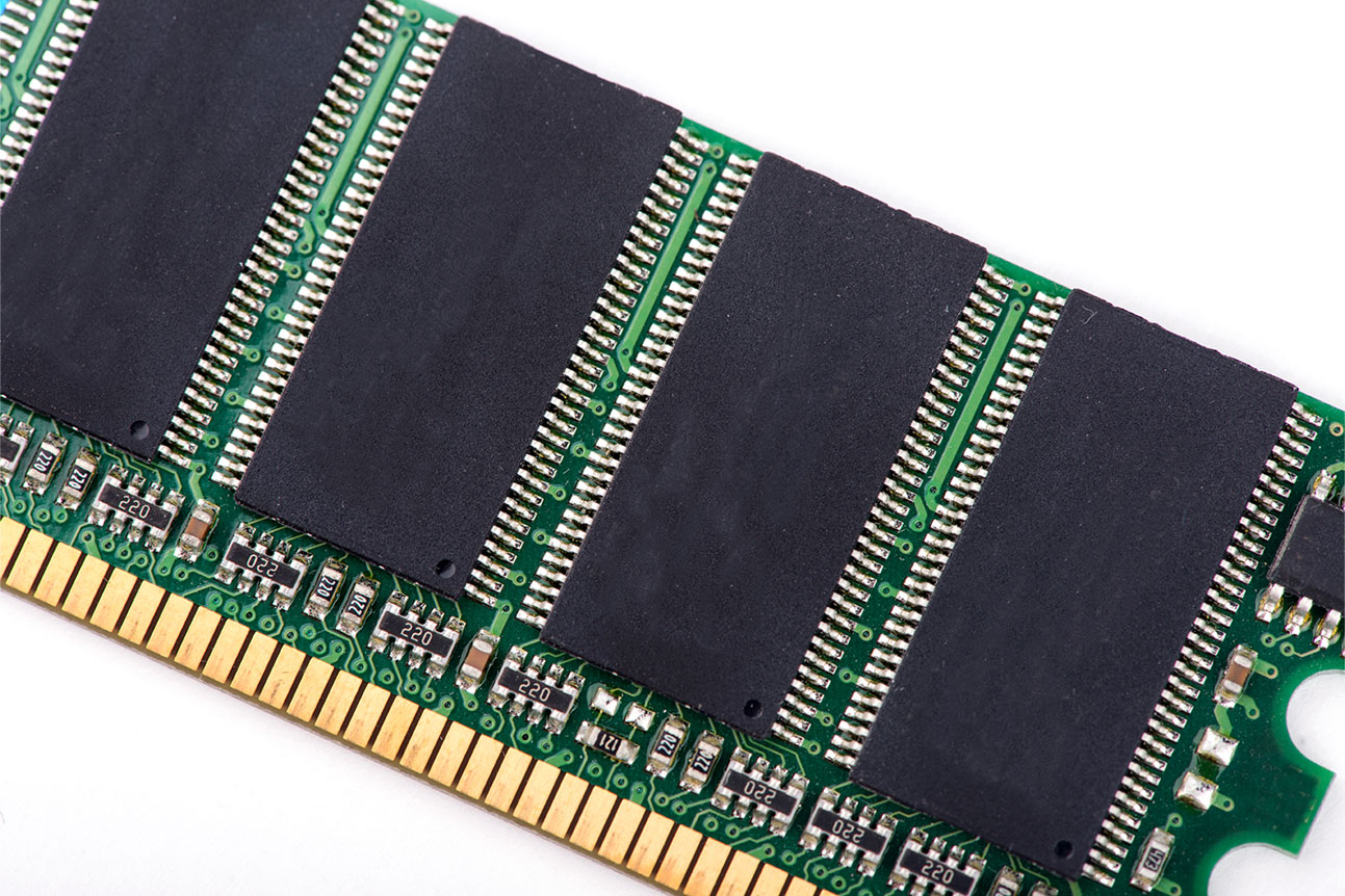
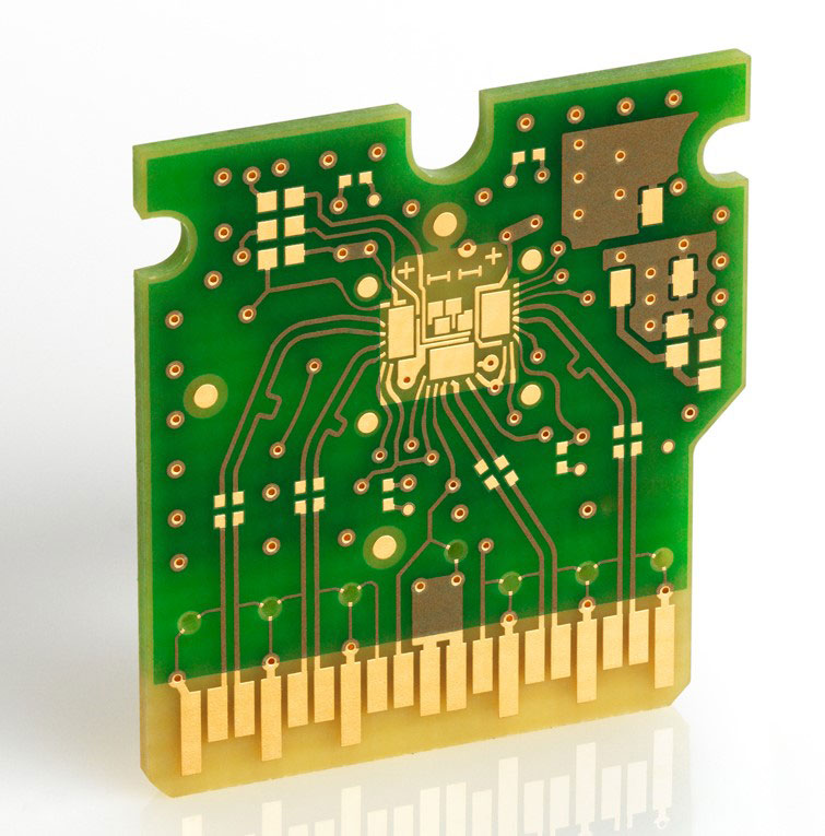
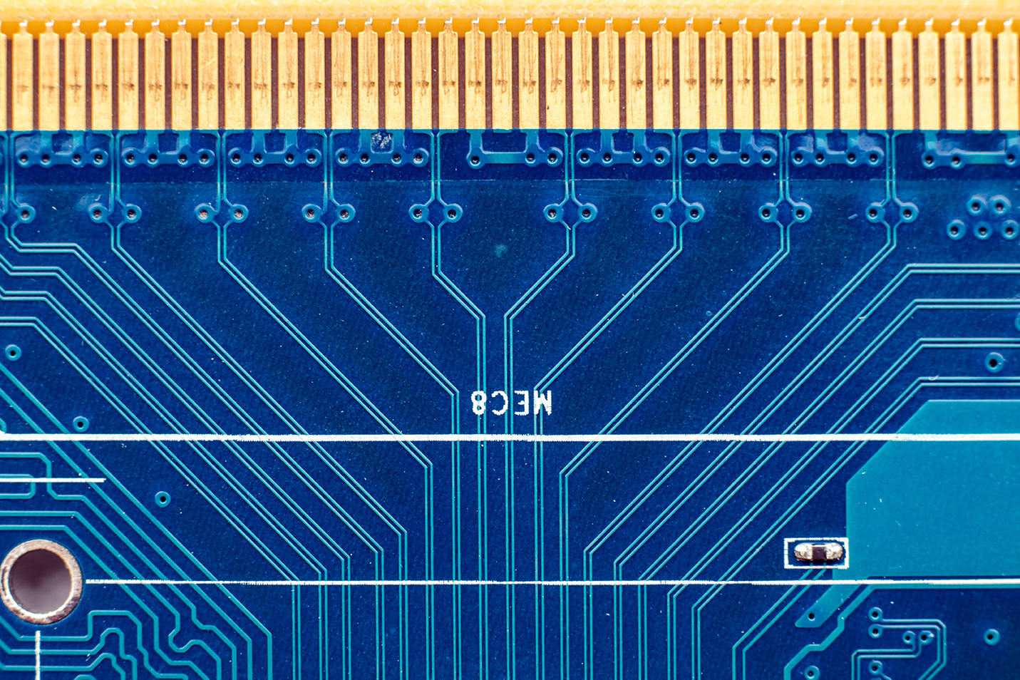
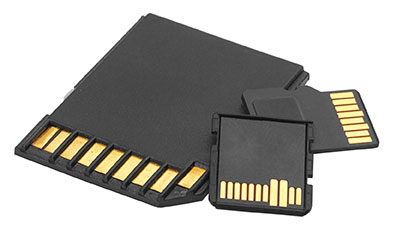
In today’s digital age, communication signals are transferred between many devices. Gold fingers, also called edge fingers, enable connections between circuit boards and other devices.
What are gold fingers/edge fingers in a PCB?
Gold fingers are gold-plated connectors found on the edge of circuit boards. They interconnect boards/electrical units using sockets. Edge fingers are used in different devices and applications such as smartphones, smartwatches, and typically in industrial applications including electronic card cages to communicate with digital signals. They protect the board connections from deterioration and failures. Edge fingers are often confused with edge connectors. However, they are used for different purposes. We will outline the distinctions in the upcoming sections.
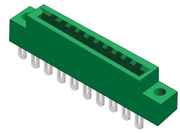
PCB edge connectors
A PCB edge connector consists of traces that lead to the board’s edge and are designed to plug into a matching socket. It facilitates the connection between two boards or from one board to an external electrical connection. These edge connectors are fairly reliable, affordable, and robust. Typically, they are used in computers as expansion slots, such as PCI Express, PCI, and AGP cards.
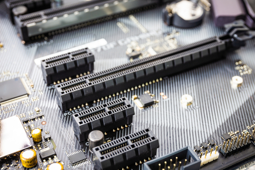
Circuit board edge connector sockets are bounded by a plastic box that is open on one side, with pins on one or both ends of the longer edges. Often, connectors contain bumps or notches for polarity and to ensure the correct device type is inserted into the connector. The socket’s width is selected according to the thickness of the connecting board. On the other side of the socket is usually an insulation-piercing connector attached to a ribbon cable. A motherboard or daughter card may also be connected to the other side.
For designing edge connectors circuit sizes, configuration, pitch, and board attach terminations are the predominant factors involved.
Connector Design Guide
5 Chapters - 32 Pages - 50 Minute ReadWhat's Inside:
- Basics
- Terminology
- Selection and layout rules
- Testing
- Application-specific PCB connectors
Download Now
Gold/edge fingers vs. PCB edge connectors
| Gold fingers or edge fingers | PCB edge connectors |
|---|---|
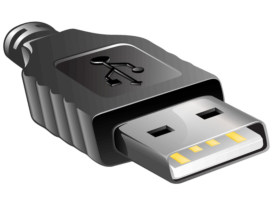
| They are used to connect PCBs to peripheral devices or the motherboard. Edge fingers creates an interface to transfer data through USB and memory cards. | They are used in computers as expansion slots (for connecting PCI Express, PCI, and AGP cards to the system bus). |
| Placed at the board edges. | Can be mounted anywhere on the circuit board. |
| They are electroplated with hard gold to increase conductivity and resistance to wear and tear. Gold fingers can be plugged in and plugged out whenever required. | Here the sockets are enclosed in a thermoplastic box, which is open on one side and has pins along the edges. PCB edge connectors are affixed permanently during the assembly process. |
| Gold fingers are designed as a pad. It is created after the solder mask preparation and needs extra milling to get the chamfered edge. | An Edge connector is configured as a pin, inserted, and soldered into the vias. |
| Feature a high-duty cycle since edge fingers can be inserted and removed multiple times. | PCB edge connectors have a lower duty cycle since they are permanently fixed once inserted |
| Manufacturing costs are higher as they involve hard gold for plating. | Less expensive, as edge connectors comprise a plastic box. |
Gold fingers not only have improved connectivity in terms of speed and cost but also offer increased reliability. While designing them, you need to give more attention to the physical dimensions of the fingers and the spacing between them while ensuring alignment precision. Both edge fingers and edge connectors are part of a single system used to connect two PCBs or a board to an electrical unit.
Gold fingers plating thickness
Gold is chosen for plating because of its high corrosion resistance, high electrical conductivity, and the ability to be alloyed with cobalt or nickel to improve its resistance to wear and tear. The thickness of the gold plating varies between 0.003 and 0.005 mil.
Electroless nickel immersion gold (ENIG)
ENIG is cost-effective and easy to solder. Since it is thin and soft (0.002-0.005 mil) it is unsuited for some boards due to abrasive effects such as insertion and removal.
Electroplated hard gold
Hard gold comes with a thickness of 0.03 mil. They can sustain abrasive effects occurring on a board due to constant usage.
Design specifications for edge fingers
- Can be easily placed on one or both sides of a board to a depth of 1 inch from the outer edge
- Should be connected with 8 mil conductor traces. It makes manufacturing easier
- Plated through-holes should not be situated close to them
- Should be kept at a distance from solder mask or silkscreen printing
- Must always face the opposite direction from the middle of the circuit board (if you want the edge to be beveled)
PCB gold finger or edge finger beveling
On a board, the edge finger plating process is performed after the application of the solder mask and before the surface finish. The plating process involves the following steps:
Nickel plating
Firstly, 0.004 to 0.008 mil of nickel is plated onto the connector edges of the fingers.
Gold plating
Later, 0.04 to 0.08 mil of hard gold is plated over the nickel. The gold is usually mixed with cobalt for increasing the surface resistance.
Edge beveling
Edge beveling is a process of creating a transitional edge between two faces of a circuit board, generally performed on the outer edge of the board. Beveling allows for smoother insertion into other PCB sockets. The edge connection pins are called gold fingers as they are gold-plated and some of them are grouped in parallel. They are available in the following versions:
- Available beveling angles: 20⁰, 30⁰, 45⁰, and 60⁰
- Residual thickness after beveling: ≥12 mil
The depth or residual thickness of the beveling can be calculated using the geometry shown below:
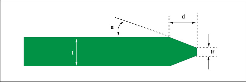
𝑑 = 𝑡 − 𝑡𝑟/ 2 ∗ sin 𝑎
Where, d = depth, 𝑎 = bevel angle, t = board thickness, and 𝑡𝑟= residual thickness.
Production standards for gold fingers
- Chemical composition: The gold plating should consist of 5-10% cobalt for maximum rigidity across the board edges.
- Thickness: The plating thickness of gold/edge fingers must fall between 0.002- 0.005 mil. The standard thickness dimensions are 3 mil, 62 mil, 93 mil, and 125 mil.
- Visual test: A visual test is conducted with a magnifying lens to ensure edges are smooth, clean, and free of excess plating.
- Tape test: It is done to check the adhesiveness of the gold plating. In this test, a strip of tape is placed along the contact edges. After removing it, the strip is inspected for traces of plating. If any gold plating is observed on the tape, then the plating lacks adequate adhesiveness.
Applications of PCB edge fingers
They have a wide range of applications in several industries including:
- Telecommunication industry: Connection for network data transfer (communication adapter)
- Computer application industry: Data transfer (laptop memory card, graphics card, etc.)
- Industrial control system: Connection to different devices (factory robot arm, high-end consumer electronics, computerized industrial machines, etc.)


