Vias are tiny conductive paths that establish an electrical connection between the different PCB layers. Learn more about PCB via design by scrolling down below.
The most reliable PCB assembly in Silicon Valley
Avoid component procurement delays by using a single vendor to source your parts. Transparent pricing. Fast turn-times.
What is the purpose of a via in PCBs?
Vias are tiny conductive paths that establish electrical connections between different PCB layers. Depending on their functionality, vias are classified as through-hole, blind, buried, and microvias. Microvias are further divided into stacked and staggered vias.
A via consists of a barrel, a pad, and an anti-pad. Barrel is a conductive tube that fills the drilled hole and a pad connects each end of the barrel to the component, plane, or trace. Antipad is a clearance hole between the barrel and the no-connect metal layer.
Also, see via covering in PCBs, such as plugging and filling, to determine the right protection method for your design.
Types of PCB vias
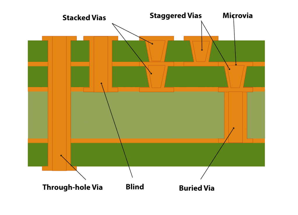
- Through-hole vias: Through-hole vias pass through the entire board from the top layer to the bottom layer. They can be either PTH (plated through-hole) or NPTH (non-plated through-hole). Learn how drills and through-hole plating are critical steps in PCB fabrication to ensure strong electrical and mechanical connections.
- Blind and buried vias: Blind via is a hole that runs from an outer layer to the inner layer but not through the entire PCB. Buried via runs between one or more inner layers. These vias provide better signal integrity, lower noise, EMI, and crosstalk due to low aspect ratios. Completely filled buried vias reduce the possibility of cracking and delamination. IPC standards depict that buried and blind vias must have a diameter of 6mils (150micrometers) or less.
- Microvias: According to IPC-T-50M, microvia is a blind structure with an ideal aspect ratio of 0.75:1. It is laser-drilled, with a diameter of less than 150μm. Its target length should not be more than 0.25mm measured from the capture land to the target land.
Microvias are generally implemented in HDI PCBs. The depth of a microvia isn’t usually more than two layers since the process of copper plating, inside these vias, is a tedious task.

Also, see castellated holes or plated half-holes for reliable board-to-board edge connections.
Why are microvias a preferred choice in HDI board design?
Microvias enhance the electrical characteristics and aids in the miniaturization of the circuit board. They enable higher routing density by reducing the layer count. This eliminates the need for through-hole vias. These vias also increase the processing power. The implementation of microvias helps to ease out the BGA breakout.
Understand why precision drills and high-quality through-hole plating are essential for reliable signal performance.
Aspect ratio for vias
Aspect ratio (AR) is the ability to effectively plate (deposit) copper inside the vias. Mathematically, AR is the ratio between the PCB thickness and the diameter of the drilled hole. It decides the reliability of a circuit board.
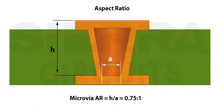
The ideal aspect ratio for a microvia is 0.75:1, and for a through-hole via, it is 10:1. You can choose more than a 10:1 aspect ratio. But it will increase the design cost, intricacies, and reliability concerns as well.
Via-in-pad
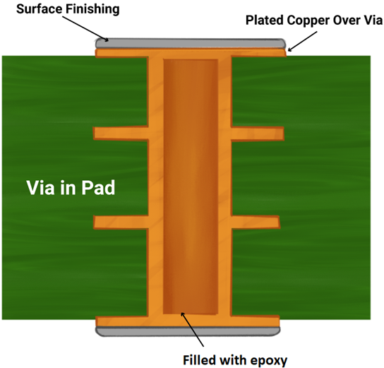
High signal speeds, large component density, and increasing thickness require the implementation of via-in-pad. PCB design engineers implement VIPPO along with the conventional via structures to meet routing and signal integrity requirements.
Advantages of VIP
- Efficient thermal management: The via-in-pad process allows the placement of vias on the flat land surface. After that, vias are plated and filled using conductive or non-conductive epoxy for the ease of thermal management. Finally, capping and plating are performed to make it invisible.
- Reduces space requirements: It also allows PCB miniaturization by reducing the space taken up by trace routing.
- VIP makes it easier to route fine pitch BGAs, which might be smaller than 32 and 40mils (0.8mm and 1mm).

Signal Integrity eBook
6 Chapters - 53 Pages - 60 Minute ReadWhat's Inside:
- Impedance discontinuities
- Crosstalk
- Reflections, ringing, overshoot and undershoot
- Via stubs
Download Now
PCB via design using EDA
When implementing vias in a PCB using an EDA, as a designer, you need to stick to the following guidelines:
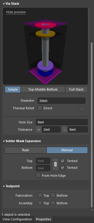
- Via creation: The first step is to create the via, by editing the dimensions of the via stack as shown in the figure above. This feature is also called a padstack editor. You can then specify the pad shape and size for various layers, and also change the tolerances, drill sizes, and more.
- PCB libraries: After creating the vias, it is useful to store the generated vias in a library feature within the EDA tool. This will make it convenient to use pre-generated vias, saving time in future designs.
- Routing tools: After designing the vias, you will need to use them during the routing stage of the board design. You can place instances of vias while routing manually or use automated routing options like fanout routers which are usually built into the EDA software.
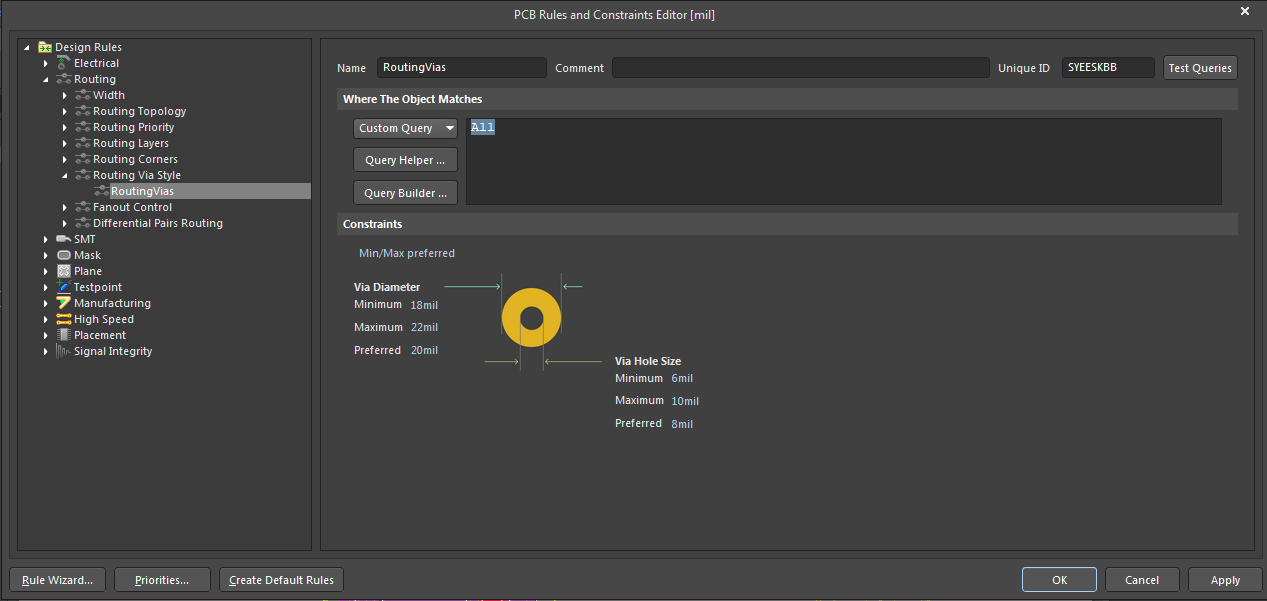
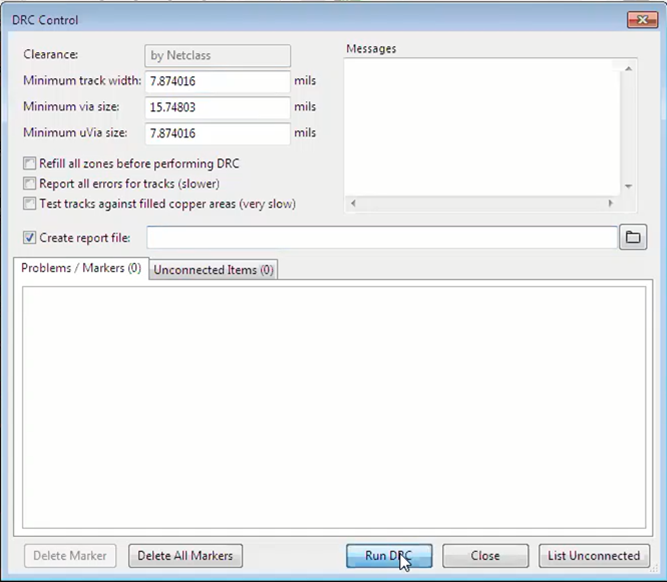
- Design rule checks (DRC): A design rule check is a set of rules used by a designer to ensure the schematic matches all the manufacturing considerations and dimensional tolerances set for a board.
To ensure that the via placement is according to design requirements, you can use the DRC feature in the EDA tool.
- Advanced features: Enhanced functionalities are aimed at elevating usage of vias to the next level. For example, the “via structures” feature will combine vias with traces, shapes, and keep-outs, to create automated fanouts that offer high-speed properties.
Sierra Circuits’ engineers and technicians have the experience to bring your PCBs to life.
PCB design tips for vias
- Opt for staggered instead of stacked vias, as stacked vias need to be filled and planarized. This process is time-consuming and requires extra cost.
- Implement controlled depth for blind and buried vias.
- Keep the aspect ratio to a minimum for high-speed vias to avoid signal reflections. This provides better electrical performance and signal integrity, low noise and crosstalk, and reduced EMI/RFI.
- Use smaller vias especially in HDI boards to minimize the stray capacitance and inductance.
- Via-in-pads must be filled unless they are present within thermal pads.
- The pad arrangement on which a BGA will be installed can use blind and through vias, provided the holes are filled and planarized. If they are not planarized, the solder joints might be compromised.
- Incorporate vias in the thermal pads under QFNs to help the solder flow to the conductive planes. These vias provide a secure solder joint for the thermal pad and hence, stop the solder from floating the package during assembly. This could compromise the solder joint quality at the QFN contacts.
- An assembly shop can compensate for a lack of through vias in a thermal pad by adding a windowpane-shaped opening in the solder paste stencil above the pad. This relieves pooling of solder and outgassing.
- Check for the minimum clearance of traces and vias from the routed/scored edges.
- Inspect the position of vias in the case of BGA packages.
- In dog-bone design, each via is separated from its pad using a predefined short trace. Check that there is no mask clearance provided for the vias present under the BGA.
- Tolerances for PCB vias include:
- Minimum outer layer annular ring and minimum inner layer annular rings are designed as per IPC standards
- Drill to plane clearance: 8mils
- Diameter: ±3mils preferred
- Location: 1mil
- Registration: 1mil
- Via clearance of solder mask: 2.5mils bigger than via pad size
- Encroachment of solder mask onto via: via size +3mils
- Anti-pad: 16mils bigger than the hole size and plane relief preferred 8mils
Via design is a critical part of design and development. Circuit board designers need to master this to execute excellent board routing strategies.
One-stop PCB assembly services, capabilities, and testing
We source components from chip manufacturers across the globe, including Mouser, Digi-Key, Arrow Electronics and others. We also warehouse a significant inventory of common parts. If we cannot source a specific component, our engineers will make recommendations for fair-price alternatives. Get started now.
