Side plating or edge plating offers solid mechanical strength and improves electrical connections. This technique also provides excellent grounding and shielding and enhances the overall reliability of your PCBs. Side plating is generally implemented in compact and high-performance applications.
Here, you’ll learn the design considerations for side plating, its manufacturing process, things to include in the fab notes, and its advantages.
What is side plating in PCBs?
Side plating is a process of adding a layer of copper along the edges of a PCB, covering the board’s perimeter from top to bottom. This technique strengthens the connection across the board, enhancing durability. You’ll often find side plating done in applications like Wi-Fi and Bluetooth modules, where robust and efficient connections are essential to avoid equipment failures.

During the edge plating process, manufacturers mill the outer edges before depositing copper. Subsequently, they apply a suitable PCB surface finish, such as ENIG, to the edges.
Why is side plating used?
Edge plating is implemented to:
- Enhance the board’s conductivity.
- Create electrical connections along the PCB’s edges.
- Protect the board from lateral shocks or mechanical stress.
- Connect secondary circuit boards to the mainboard through edge connections.
- Solder the edges to improve assembly quality and durability.
Benefits of edge plating
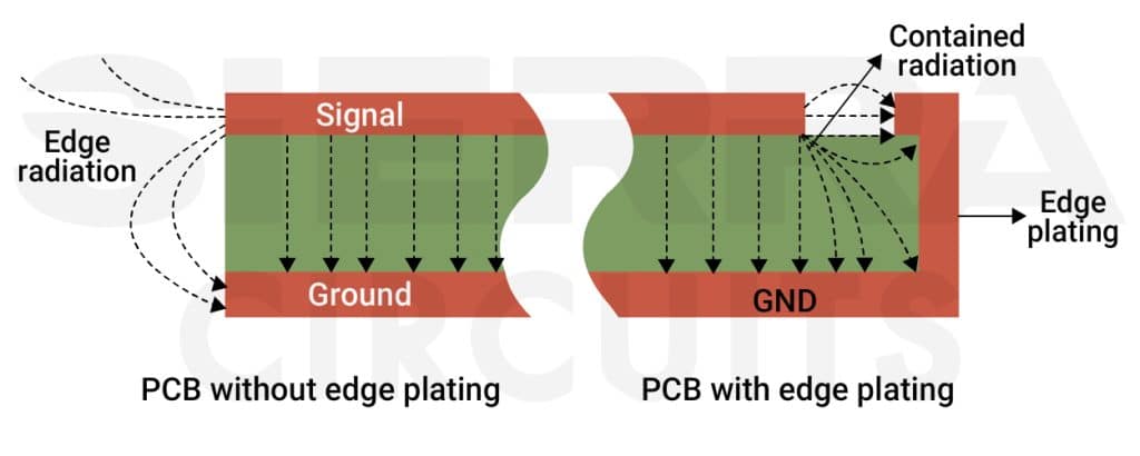
- Edge plating, when connected to the ground, creates a Faraday cage around the board’s perimeter. This cage significantly reduces EM emissions from the board.
- Protects the internal circuitry from external EMI, and this shielding is crucial for meeting EMC regulations.
- Prevents electrostatic damage that can occur during handling.
- For RF designs housed in metal enclosures, edge plating provides superior electrical contact between the PCB and the enclosure offering enhanced grounding.
- For edge-mounted connectors (like some RF connectors), edge plating provides a better ground connection.
- Provides a low-impedance return path for high-frequency signals, which can reduce signal reflections and crosstalk in PCBs.
- Contributes to better heat dissipation by providing an additional path for heat to escape the board when connected to internal ground planes or mounted in a conductive chassis.
- Improves electrical and mechanical connections between boards.
- Protects vulnerable edge connections and offers additional mechanical strength to PCB edges, beneficial for applications subjected to mechanical stress or frequent handling.
- In applications exposed to moisture or corrosive environments, edge plating can provide an additional layer of protection for the PCB substrate.
If your board includes card-edge connectors, our comprehensive gold fingers guide covers design rules and plating best practices to ensure long-term performance.
Side plating Vs castellated edges
The table below summarizes the difference between side plating and castellated holes.
| Side/edge plating | Castellated edge |
|---|---|
| Metallization of the PCB edge with copper for better electrical connectivity. | Features plated half-holes along the PCB edge. |
| Enhances electrical connections, provides EMI shielding, improves structural rigidity, enables edge connections, aids grounding, and reduces board failure risk. | Facilitates board-to-board connections without extra components and simplifies assembly. |
| Coated with a copper layer through the process of electroless plating, followed by electroplating. | PTHs are created first, followed by milling to form castellated half-holes. |
| Used in applications demanding robust electrical connections, particularly in high-frequency circuits and systems requiring edge-to-edge board connections. Applications: WiFi and Bluetooth. | Commonly used in modular designs where components need to be easily attached or detached from the main board, enhancing flexibility in circuit design. Applications: Embedded systems and modular PCBs. |
Also, see plated-through slots to properly accommodate rectangular leads and improve mechanical and electrical reliability.
How to implement edge plating in your PCB layout
Follow these steps to incorporate side plating in your EDA tool:
Step 1: Define the copper overlap
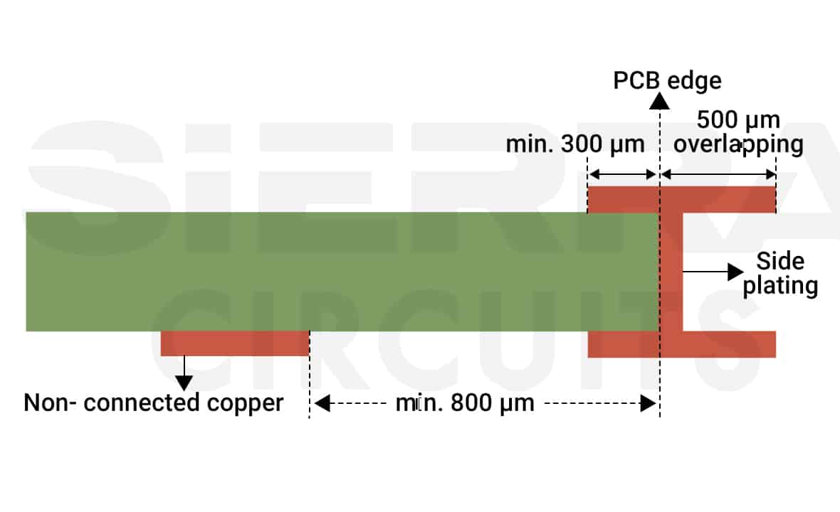
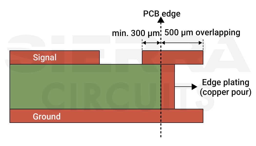
As a PCB designer, use overlapping copper (surface, pads, or tracks) to define the plated area along the edge in the CAD layout. Ensure a minimum overlap of 500 μm.
For connected layers, maintain at least 300 μm of connected copper.
For non-connected layers, keep a minimum gap of 800 μm from the outer contour.
Alternatively, you can completely wrap a polygon pour layer around the entire edge of the PCB and connect it back to another surface layer.
Step 2: Verify ground layer connections
Ensure ground planes on top, bottom, and internal layers (if applicable) are linked for improved shielding and performance.
Download our eBook to learn how to design for manufacturing.

Design for Manufacturing Handbook
11 Chapters - 96 Pages - 90 Minute ReadWhat's Inside:
- Annular rings: avoid drill breakouts
- Vias: optimize your design
- Trace width and space: follow the best practices
- Solder mask and silkscreen: get the must-knows
Download Now
17 PCB design considerations for side plating
- For boards with internal power planes, use design rules to maintain proper clearance between these planes and the board edges or cutouts. This ensures there is no unintentional connection between power planes and edge plating.
- Maintain a minimum clearance of 10 mil between the edge plating and other copper features. Always check with your manufacturer before finalizing these values.
- For non-grounded edge plating, ensure there is adequate isolation from the signal traces to prevent unintended coupling or short circuits.
- Avoid placing vias near the board edges. Consult your CM if you’re placing a plated hole near the edge plating.
- Ensure edge plating doesn’t interfere with edge-mounted connectors such as SMA. You need to create cutouts in the plating to mount these components.
- If castellated holes are present in your design, edge plating must wrap around these holes to provide solder points for mounting on baseboards.
- If any planes need to connect to the side-plated area, they should extend beyond the PCB edge.
- To ensure proper grounding and shielding, remove the solder mask from areas where edge plating will contact shielded enclosures.
- Define areas where you should pull back the solder mask from the edge to expose the plating. A typical pullback might be 20-50 mil.
- Ensure solder mask openings are consistent on both the top and bottom layers.
- If using edge plating for thermal management, consider connecting it to internal ground planes with thermal vias.
- For high-speed or RF designs, consider how edge plating affects controlled impedance traces near the board edge. You may need to adjust trace widths or increase their distance from the edge to maintain the desired impedance.
- Ensure there are anchor strips along the external top and bottom edges, as it serves as a mechanical connection point for the side plate. This securely attaches the side plate to the PCB.
- Ensure copper polygons intended to connect to the edge plating extend to the very edge of the board or cut out on all layers where they merge. In some cases, manufacturers may require the polygons to overlap the edges of the PCB or cutouts.
- To plate all four edges, provide 3-4 short unplated segments (at least 3mm apart) for panel support tabs.
- Place 1-2 mm jumpers in non-critical areas to hold the board during copper deposition. After plating, these jumpers are cut, leaving non-plated areas. Specify jumper locations or include them in the production files.
- Leave space for panel tabs that hold the board in place during plating within a multiple-up array, which will later be broken off after assembly.
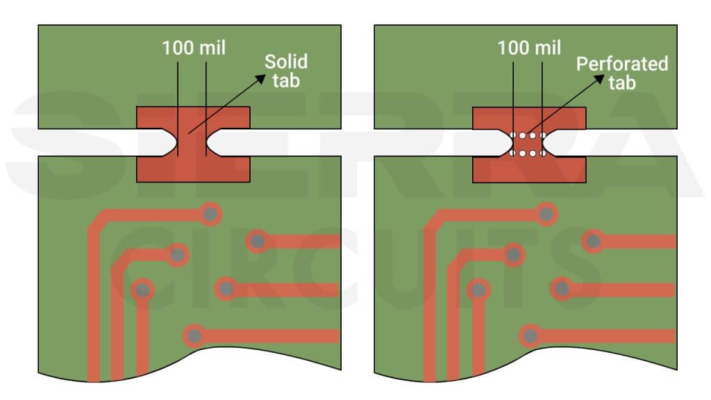
In the above image, you see two types of tabs: perforated tabs (left) and solid tabs (right). Perforated tabs (mouse bites) are broken off after assembly, while solid tabs are removed during the final fabrication stage using a router, leaving a small protrusion along the edge.
-
- A tab can be placed at the interruption point; this tab prevents plating in that specific area. After plating, remove the tab. Use this method for interruptions larger than 0.200 inches.
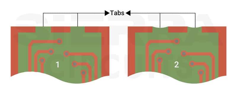
- Place tabs for plating interruptions.
-
- Apply the plating continuously along the edges, and then use a router to remove the plating at specific points. This process leaves a small tab or indentation in the circuit, as shown in the above image (2). Use this method for interruptions smaller than 0.200 inches.
- Avoid placing tabs near critical components, high-speed signals, or areas prone to mechanical stress.
- The tabs between the board and panel should have a thickness of about 2.5 mm or 100 mil. Thicker tabs offer better adhesion.
- During de-tabbing, ensure that the artwork surrounding the tabs on both the outer and inner layers is free of metal. Aim for a minimum gap of 25 mm/10 mil between the copper layer features and the tabs.
Sierra Circuits specializes in high-quality PCB fabrication with advanced features like side plating. To learn more, visit PCB manufacturing capabilities.
Required fab notes for edge plating
If your design requires edge plating, make sure you include these details in your fab notes:
- Specify which board edges require plating. To plate specific edges, provide a clear diagram with markings.
- If any planes need to connect to the side-plated area, add a note in the fab drawing specifying the layers.
- Mention the location of the side plating and the desired surface finish on a mechanical layer.
- Indicate the areas that require side-plating and specify the desired copper thickness.
- If you’re using jumpers, clearly specify their locations.
Step-by-step side plating manufacturing procedure
- Before plating, the board edges are milled, cleaned, degreased, and roughened to ensure proper adhesion of the plating materials. This step eliminates contaminants and ensures uniform plating coverage.
- The PCB undergoes a two-part plating process. Initially, a precise electroless copper plating bath evenly applies a thin copper layer on the board, including the edges. This layer acts as a conductive base for future plating.
- The board moves on to the electrolytic copper plating process, where a thicker copper layer is carefully formed along the edges.
- Excess copper is removed through chemical etching. This results in the desired copper layout on the board, including the plated edges.
- Board edges undergo a surface preparation process like micro etching. This removes any surface oxides or contaminants, improving adhesion and ensuring full plating coverage.
- Manufacturers apply an additional finish, such as ENIG, to the plated edges. This improves solderability, corrosion resistance, and overall durability.
- The boards are cleaned and dried to remove any residual chemicals or debris from the plating process.
- After plating, the manufacturer cuts the panel to separate the printed boards, leaving the plated edges intact. This step is critical in maintaining the integrity of the plated sections during the separation process.
- Detailed inspection is performed to ensure the plating meets the required specifications for thickness, continuity, and adhesion. Address any defects or inconsistencies before final testing.
PCB edge plating improves the durability and reliability of printed circuit boards by metalizing the edges, preventing oxidation and corrosion. This process ensures consistent electrical conductivity and creates strong, reliable connections with mating components.


