What is a PCB stencil?
The assembly of surface-mount devices (SMDs) on PCBs requires a stencil. To solder the components on a circuit board, it is necessary to apply solder paste on the component footprints. To accomplish this, SMD stencils are used.
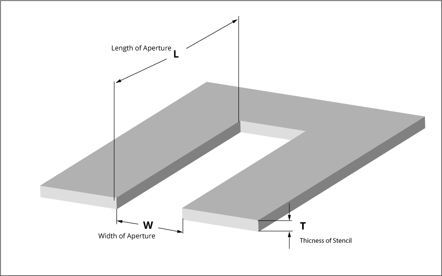
An SMD stencil or a PCB stencil is a thin stainless steel foil that is placed on the top surface of the board with openings at the SMD device locations. Then solder paste is applied over the stencil and it gets transferred onto the component pad through the holes in the stencil.
Solder paste printing is a crucial process during the SMD assembly. It is used to spread the solder paste on the bare circuit board before mounting the components.
Laser is used to cut the stencils at the location of the surface-mount components. Later, the solder paste is applied to the board through these apertures. Before the use of stencils, wire mesh screens were used for this process. When solder paste was pushed through the wire mesh, it limited the aperture sizes, stencil life, and print speed. Hence, the introduction of stencils has overcome these limitations.
What is the stencil process?
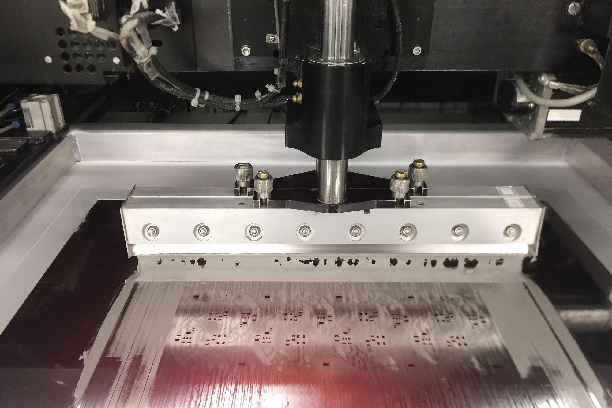
The first step in solder paste printing is aligning the stencil on the PCB. The whole process is automated and is carried out using printers. Once the board is loaded into the printer, the internal vision system makes sure that the stencil is aligned properly with the board. This is done by making use of the global fiducials as the reference.
After the stencil is properly aligned on the circuit board, solder paste is applied to all the openings. This is done using a metal squeegee blade. Then the stainless steel foil is removed from the board, and the solder paste gets deposited. All the SMD components are placed afterward.
The most reliable PCB assembly in Silicon Valley
Avoid component procurement delays by using a single vendor to source your parts. Transparent pricing. Fast turn-times. Learn more about our assembly services here.
How thick is a solder stencil?
The thickness of a stencil is equal to the a solder paste height of 0.006 to 0.010 inches. The thickness should not be too thick as it would affect the transfer of the solder paste to the board surface. Surface tension will cause the paste to stick to the insides of the stencil apertures if they are too thick. A designer should consider all these facts while deciding the thickness of the stencil.
Transfer efficiency of SMD stencils
The working of a stencil is determined by its transfer efficiency. How well does the solder paste get transferred to the circuit board surface through the apertures in the stencil? This is the main concern while designing and choosing stencils.
Ideally, the amount of solder paste applied to the aperture should be transferred completely to the PCB surface. But in reality, the volume of solder paste deposited will differ from the calculated volume. This ratio is termed as the transfer efficiency and is given by:
Transfer efficiency=Volume of printed deposit/Theoretical maximum volume
The theoretical maximum volume is the same as the volume of the stencil aperture. The ideal value of transfer efficiency is 1. But in practicality, this value will be less than that. The focus is more on making the value as close to 1 as possible to attain maximum transfer.
Get started with printed circuit board assembly
Sierra Circuits is capable of assembling BGA, micro-BGA, QFN and other leadless package parts. Whether you need 1 or 10,000 boards assembled, we make it easy for your project to come to life.

PCB Design for Assembly Handbook
6 Chapters - 50 Pages - 70 Minute ReadWhat's Inside:
- Recommended layout for components
- Common PCB assembly defects
- Factors that impact the cost of the PCB assembly, including:
- Component packages
- Board assembly volumes
Download Now
What are SMT stencils made of?
In general, stencils are made of stainless steel. Nickel is also used to manufacture stencils rarely. It depends on the method of manufacturing that is adapted. The widely used method is explained below.
Laser-cut stencil
Laser-cut stencils are SMD stencils with apertures created by means of a laser. Usually, stencils are made up of stainless steel. The laser method of manufacturing stencils offers a lot of advantages such as high precision and short processing time. This method also exhibits high accuracy while creating apertures.
Advantages of laser-cut stencils
The aperture walls cut out by laser are given an electro-polishing or nickel plating for a better finish. Since the laser cutting method does not require any photo films, the process becomes somewhat less complicated. Also, the ability of this method to create identical apertures as compared to others makes it more reliable.
The apertures created using this method are trapezoidal in shape. The trapezoidal apertures are known for better solid paste release characteristics.
E-FAB
An electroforming (E-FAB) nickel process is used tomanufacturie stencils. This process creates smooth tapered aperture walls. The E-FAB process also results in creating a ridge at the bottom of the stencil that will help to increase the transfer efficiency.
Once the stencils are used, they should be thoroughly cleaned to get rid of any solder paste remnants. These stencils are then stored in a protective environment and are properly checked before usage.
One-stop PCB assembly services, capabilities, and testing
We source components from chip manufacturers across the globe, including Mouser, Digi-Key, Arrow Electronics and others. We also warehouse a significant inventory of common parts. If we cannot source a specific component, our engineers will make recommendations for fair-price alternatives. Get started now.


