


Contents

On-demand webinar
How Good is My Shield? An Introduction to Transfer Impedance and Shielding Effectiveness
by Karen Burnham
Designing high-speed PCBs is crucial to support real-world applications. Signal transmission problems are prominent when a PCB deals with high-speed signals. An excellent high-speed board integrates various components and routing while avoiding signal integrity issues. The three main challenges we face in high-frequency boards are signal integrity, EMI/EMC, and dielectric loss.
Highlights
- Implement impedance matching techniques to prevent signal distortion and reflections
- Minimize ground bounce in high-speed PCBs by adopting pin slew rate control, providing multiple power and ground pins, and utilizing larger vias for decoupling capacitors.
- Implement parallel, thevenin, active, series-RC, series, and differential pair termination techniques to ensure efficient signal transmission.
- Optimize component placement, trace routing, and ground plane design to minimize electromagnetic interference and achieve electromagnetic compatibility for high-speed PCBs.
In this blog post, we will be discussing the following factors that require attention while dealing with high-speed signals in a PCB design
What is a high-speed signal in a PCB?
Signals with frequencies ranging from 50 MHz to as high as 3 GHz are considered high-speed signals, such as clock signals. Ideally, a clock signal is a square wave, but it is practically impossible to change its ‘LOW’ level to ‘HIGH’ level (and vice versa) instantly. It has a specific rise and fall time, due to which it appears to be a trapezoid in the time domain. It is worth noticing that the amplitude of the higher frequency harmonics of the clock signal in the frequency domain depends upon its rise and fall time. If the rise time is longer, then the magnitude of the harmonics will become smaller.
Why do signal distortions occur at high frequency?
At low frequencies (>1kHz), the signals remain within the data characterization limits, and the system performs as intended. When speed increases, the higher frequency impact comes into play, resulting in ringing, crosstalk, reflections, ground bounce, and impedance mismatch issues. It affects not only the digital properties of the system but the analog properties as well. These issues are more prone to increasing data rates for I/O and memory interfaces. Practically, these issues can be avoided by employing advanced PCB design services or by following strict layout guidelines. The signal routing, termination schemes, and power distribution techniques can help the designers to realize an effective PCB.
Read our blog post, 5 typical PCB design challenges with solutions for engineers, to learn more about common PCB design issues and how to address them.

Why consider signal integrity in high-speed PCB design?
Signal integrity: Ideally, in a PCB, a signal should travel from a source (Tx) to a load (Rx) unimpaired/ unadulterated. But practically, it does not happen. The signal reaches the load with some losses (impedance mismatch, crosstalk, attenuation, reflection, and switching issues). Signal integrity (SI) is the term defined to measure these signal distortions in the high-frequency regime. Signal integrity helps to predict and understand these critical issues by providing practical solutions.
High-speed PCB design requires visualizing traces as transmission lines instead of simple wires. Identification of the highest operating frequency in the design helps to target the traces that should be treated as transmission lines. If the traces exceed about 1/10 of the wavelength of that frequency, then they can be treated as transmission lines. These transmission lines require digital as well as analog analysis.
PCB substrate: Substrate material used during the PCB construction contributes to signal integrity problems. Each PCB substrate has a different relative dielectric constant (εr) value. It determines the length at which the signal traces must be considered as transmission lines, and of course, in such scenarios, the designers need to take care of signal integrity threats.
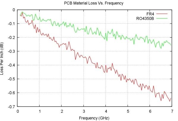
Using the εr value, designers can evaluate the velocity (Vp) at which the signal flows and propagation delay (tPD). These parameters help to determine the length at which the trace should be considered a transmission line. The graph below depicts how insertion loss increases with signal frequency. The insertion loss (per inch) is measured for FR-4 (glass epoxy) and high-frequency Rogers RO4350B material. Higher insertion loss may lead to more attenuation. Click here for more insight on PCB materials and laminates.

High-Speed PCB Design Guide
8 Chapters - 115 Pages - 150 Minute ReadWhat's Inside:
- Explanations of signal integrity issues
- Understanding transmission lines and controlled impedance
- Selection process of high-speed PCB materials
- High-speed layout guidelines
Download Now
7 parameters to consider for signal integrity in high-speed PCB designs
1. Impedance matching
This parameter is important for faster and longer trace runs. The three factors that affect impedance control are substrate material, trace width, and height of the trace from the ground/power plane.
At low frequencies, a PCB track is defined by its DC characteristics. It can be considered as an ideal circuit, devoid of resistance, capacitance, and inductance. When frequency rises, inductance and capacitance associated with the track start impacting its performance. Impedance mismatch in traces due to via stubs and imperfections in traces don’t allow the signal to be fully absorbed within the receiver (load); that’s why the extra energy is reflected towards the transmitter (source). This process repeats again and again until all the energy is absorbed. At high data rates, it causes signal overshoot, undershoot, and ringing, which generates signal errors. To solve this problem, these transmission lines are provided with ground planes underneath them and termination resistances.
It is important to calculate the impedance of the line. (It is calculated by combining the line thickness, the dielectric constant of the board, and the distance between the line and the ground plane.) Sometimes, the transmission line needs to traverse between different layers, and therefore, the distance between the line and the ground plane changes. In such a case, the line impedance can be maintained at the same value by changing the line thickness.
Note: For high-frequency, high-speed designs, PCB tracks are considered transmission lines.
1.1 Impedance control measures in high-speed PCB design
Impedance mismatch can be controlled by implementing adequate termination schemes. The selection of the termination scheme depends upon the application. Let us discuss some of them.
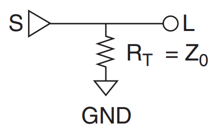
1.1.1 Parallel termination scheme: In this scheme, the termination resistor (RT) is equal to the line impedance. This termination resistor is placed as close to the load as possible for maximum efficiency. The current loading of this termination resistor is maximum at a high-output state.
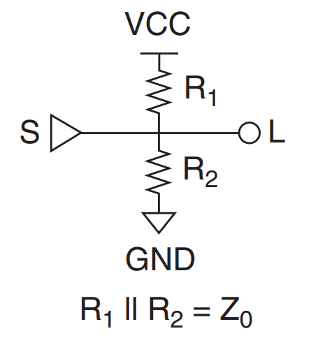
1.1.2 Thevenin termination scheme: It is an alternative to the parallel termination scheme, where the terminating resistor (RT) is split into two separate resistors, which is equal to the line impedance (when combined). This scheme reduces the total current draw from the source and adds current drawn from the power supply because the resistors are placed between VCC and ground.
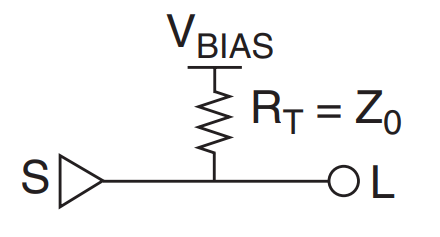
1.1.3 Active parallel termination: Here, the terminating resistor equal to the line impedance (Z0) is placed in the path of bias voltage. The bias voltage is arranged so that the output drivers can extract current from both high and low-level signals. This technique requires a separate voltage source that can sink and source currents to match the output transfer rates.
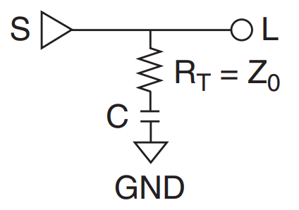
1.1.4 Series-RC parallel termination: In this scheme, the resistor and capacitor (>100pF) combination act as terminating impedance. Here, the terminating resistor (RT) is equal to Z0 and the capacitor blocks the low-frequency signal components and passes the high-frequency components. So, the DC loading effect of RT does not impact the driver.
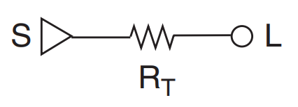
1.1.5 Series termination: It matches the impedance at the signal source instead of matching it at the load. This scheme helps attenuate secondary reflections. The line impedance varies depending on the distribution of the load. Therefore, a single resistor value does not apply to all conditions. This method requires only a single component at the source rather than multiple components at each load but delays the signal path by increasing the RC time constant.
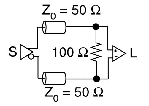
1.1.6 Differential pair termination: It requires a termination resistor between the signals at the receiving device. The termination resistor must match the differential load impedance (typically 100Ω).

2. Attenuation
A high-frequency transmission medium makes it difficult for the receiver to interpret the correct information. The following transmission losses occur due to transmission media:
Dielectric absorption: The signal in the high-frequency medium causes the PCB dielectric material to absorb signal energy. It reduces the signal strength. It can only be controlled by choosing a perfect PCB material.
Skin effect: High-frequency signals are also responsible for generating waveforms with varying current values. Such signals have their self-inductance values, which initiate an increased inductive reactance at high frequencies. It is responsible for the reduction in the conductive area on the PCB surface, more resistance, and attenuation in the signal strength. The skin-effect can be reduced by increasing the track width but it is not feasible always.
2.1 Attenuation control in high-speed PCB design
Along with a careful selection of PCB insulator material and track layout, signal attenuation can also be reduced by including programmable differential output voltages, pre-emphasis, and receiver equalization. Increment in the differential output voltages helps to improve the signal at the receiver. Pre-emphasis is the way of only strengthening the high-frequency signal component by increasing the level of the first transmitted symbol. Receiver equalization circuitry attenuates the low-frequency signal components to cover the transmission line losses.
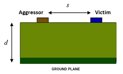
3. Crosstalk
Being electronic industry enthusiasts, we all know when current, say signal, travels through a wire it generates magnetic fields around its vicinity. If two wires are nearby, then there is the possibility that the two magnetic fields will interact, causing energy cross-coupling between two signals called crosstalk.
Prominently, inductive coupling (current induced by the magnetic field from the source wire on the idle wire) and capacitive coupling (coupling of the electric field when the idle wire is exposed to the amount of current proportional to the rate of change of voltage in the source wire) are responsible for energy cross-coupling leading to crosstalk.
Crosstalk is of two types; vertical and horizontal. Vertical crosstalk is caused by signals on the other layers or inter-layer, while signals on the same layer or intra-layer are responsible for horizontal crosstalk.
Note: The maximum crosstalk value is the difference between the expected voltage at the receiver and the receiver threshold.
3.1 Crosstalk control in high-speed PCB design
Crosstalk can be prevented by separating the traces, placing ground planes between the layers, and using low-dielectric material.
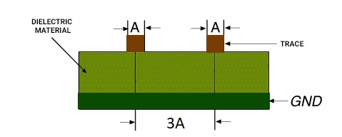
3.1.1 Traces separation: The center-to-center separation between the two traces should be at least 3 times their trace width. Without disturbing the separation between two traces, reducing the distance between the trace and the ground plane up to 10 mils helps in mitigating the crosstalk.
3.1.2 Placement of solid ground planes: Crosstalk between different layers can be prevented by placing solid ground planes between them. Though adding planes increases cost, they resolve SI problems like controlling trace impedance, reducing bypass capacitor current loop, and power supply impedance, etc.
3.1.3 Low dielectric constant material: Material with low dielectric constant overcomes crosstalk by reducing the mutual capacitance/stray capacitance between traces.
4. Impact of vias
Via location affects the signal integrity by increasing reflections, crosstalk, and changing the impedance values.
- Vias are important for routing, but including them adds to the inductance and capacitance values. This changes the characteristic impedance value, increasing reflections.
- Vias also add to the trace length. Refrain from adding vias in different traces.
5. Routing techniques
- Orthogonal routing to direct signal on different layers and to minimize the coupled region.
- Minimize parallel run lengths between signals. Route with short parallel runs only.
- Reduce drive fanout (number of loads)
6. Switching effects: Ground bounce
Unlike analog, digital circuitry requires fast on-off time since it works on switching between ‘0’ and ‘1’ and ‘1’ and ‘0’ signal levels. When speed increases, the switching period decreases. When several outputs switch simultaneously from ‘HIGH’ logic to ‘LOW,’ the charges stored in the I/O load capacitances flow into the device.
This current exits the device through the internal ground through pins that have impedance onto the ground. The switching current develops a voltage in this impedance. Thus, there is a voltage difference between the device and the board ground.
This voltage difference is known as ground bounce. The ground bounce causes a ‘LOW’ output to be seen as ‘HIGH’ by other devices on the board. Ground bounce can be reduced by adopting solutions like:
- Pin slew rate control (allows the designer to slow down the driver so that the bounce rate can be reduced). Fast slew rate is responsible for reflection, crosstalk, and ground bounce; that’s why its reduction is a must.
- Provide multiple power and ground pins (allow locating a high-speed I/O pin close to a ground pin to mitigate the switching effects).
6.1 Design considerations for ground bounce reduction in high-speed PCB
While dealing with high-speed signals in a PCB, a designer should consider the following design considerations:
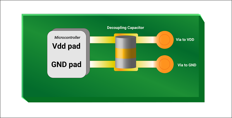
- Add decoupling capacitors for the corresponding VCC/GND pair. Add the decoupling capacitors as close as possible to the supply and ground pins of the device. If the power and GND come to the pins through vias then the decoupling capacitor should be placed between the pins and the vias.
- Add external buffers at the output to minimize the loading on device pins.
- Control the load capacitance by buffering loads with an external device, such as a buffer IC.
- Minimize the number of outputs that can switch simultaneously and distribute them uniformly throughout the device.
- Remove pull-up resistance wherever possible (use pull-down resistors).
- Use multi-layer PCBs that provide separate VCC and ground planes.
- Develop synchronous designs. Such designs will not be affected by instantaneous pin-switching.
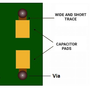
- Implement a bigger via size to connect the capacitor pad to the power and ground plane to reduce the inductance in decoupling capacitors.
- Place the via close to the capacitor pad.
- Use surface-mount capacitors to minimize lead inductance.
Note: System noise can be reduced by providing uniformly distributed power through power planes.
Also read: The Pros and Cons of Composite Amplifiers
7. EMI
PCBs also affect the EMI/EMC performance of the system. Auto-routed boards generally abide by the design rules (DRC) and do not meet the electromagnetic compatibility requirements.
That’s why it’s always advised to ensure that components are properly placed and traces are optimally routed. It helps to realize products that fulfill all electromagnetic compatibility and signal integrity requirements on time within the given budget. Designing an electromagnetic-compatible PCB can improve the overall system’s performance. Learn more about PCB design guidelines for EMI and EMC.
Every PCB is susceptible to electromagnetic interference. It can be reduced through the following ways:
- Use low-inductance components, like surface mount capacitors, which have low ESR and effective series inductance (ESL).
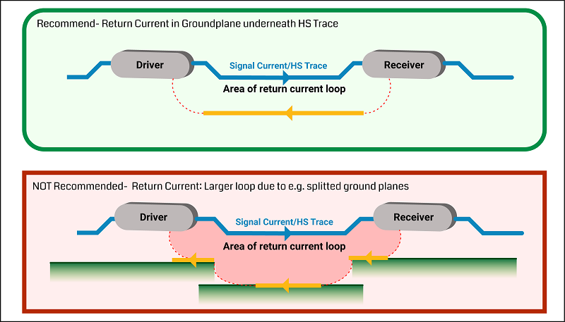
- Provide proper grounding to achieve the shortest current return path and the shortest current loops.

- Always use solid ground planes next to the power/signal planes.
To understand the role of return paths in maintaining SI in connectors, see how to assemble connectors and cables for signal integrity.
Quick tips for high-speed PCB designers
- Identify the highest frequency net and calculate the fastest rise time in the system.
- Check the electrical specifications at the inputs and outputs of the sinks and sources.
- Think about controlled impedance values, termination, and propagation delay on a trace. Read why controlled impedance really matters?
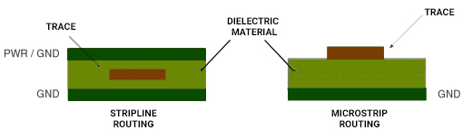
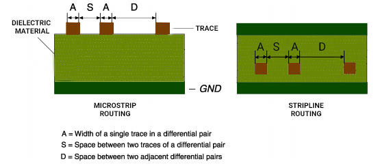
- Choose between microstrip (refers to a trace routed on an outside layer of the PCB separated by a dielectric from the reference plane (GND or VCC) and stripline (refers to a trace routed on an inside layer with two reference planes) routing techniques. Simulate to identify which method is more EMC-compliant and can give better signal integrity results.
- For quality signal transmission, consider clock and differential routing techniques.
- Think about the number of different supply voltages. Do they have their power plane?
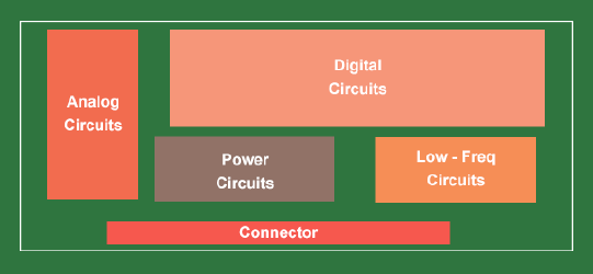
- Create a diagram for functional groups like transmitter path, receiver path, analog signals, digital signals, etc.
- Is there any interconnection between at least two independent functional groups? Pay attention to them and always consider the return current and crosstalk to other traces.
- Think about space width clearance.
- What should be the minimum distance between the two layers?
- What are the minimum Drill and Via requirements? Is it feasible to use blind and buried vias?
For expert insights into high-speed and HDI designs, see high-speed and HDI PCB design strategies by Syed Ubaid Ali Warsi
High-speed PCB materials
The most commonly used laminate material is FR-4. It is very cost-effective as long as the board frequencies kept in the range from 2.5 to 3 GHz. At high speed, materials like Rogers RO4350 have better properties than the FR-4. The only trade-off is cost. Non-FR-4 materials are expensive.
The velocity of the signal traveling through the PCB depends upon the dielectric constant of the PCB. Let’s have an example: when frequency surpasses 5 GHz, the dielectric constant of FR-4 (4.7) drops to 4.
On the other hand, the dielectric value of Rogers RO4350 remains constant (around 3.5) till 15 GHz. If the dielectric constant of the PCB keeps on changing with the frequency, then different frequency components of the signal will acquire different velocities and will reach the load at different times, resulting in signal distortion.
To learn about highly reliable materials that can be used in your high-speed applications, see OhmegaPly and TCR Materials with Embedded Passives Technology in PCB Manufacturing
High-Speed Material Design Guide
6 Chapters - 19 Pages - 30 Minute ReadWhat's Inside:
- Importance of choosing the right material for your high-speed design
- Parameters that affect material selection
- Effect of dielectric constituents on your circuit board
- Characteristics of high-speed materials
- Effect of resin content and glass weave structure on your PCB
Download Now
Why is it important to include design simulations and checks in high-speed PCB design?
Signal integrity checks are essential to maintain design transparency. If it’s not performed during the design, then it cannot be eradicated once the board has been built. In view of this, the PCB design software comes with a signal integrity check so that the PCB layout can be optimized to minimize errors. Do you want to learn more about how to simulate a channel to identify and resolve signal integrity problems? Watch our tutorial with Keysight on the basics to solve signal integrity problems.
Key takeaways
- Materials with low dielectric constants (<4) can reduce crosstalk by reducing the mutual capacitance/stray capacitance between traces.
- Solid ground planes should be used next to power/signal planes to resolve signal integrity problems.
- Design simulations and checks are crucial for optimizing PCB layouts and minimizing errors.
- Various termination schemes like parallel termination, Thevenin termination, active parallel termination, series-RC parallel termination, series termination, and differential pair termination help manage impedance and signal integrity.
- Attenuation in high-speed PCBs can be reduced by including programmable differential output voltages, pre-emphasis, and receiver equalization.
- Crosstalk, caused by inductive and capacitive coupling between signals, can be mitigated by separating traces, using solid ground planes, and employing low-dielectric material.
- Different routing techniques like orthogonal routing, minimizing parallel run lengths, reducing drive fanout, and considering clock and differential routing are important for high-speed PCB design.
- Ground bounce, resulting from fast switching between ‘0’ and ‘1’ signal levels, can be reduced through pin slew rate control, providing multiple power and ground pins, decoupling capacitors, and synchronous designs.
- Signal integrity checks during design are crucial to identify and eliminate factors degrading signal quality, with PCB design software offering tools for optimization and error minimization.
- High-speed PCB design requires careful consideration of signal frequency, termination, impedance, routing techniques, and material properties to ensure reliable performance.
In high-speed designs, signal integrity and EMC understanding and implementation during design play an important role. Signal integrity is all about identifying and eliminating factors responsible for degrading a signal’s quality when it travels through a medium from one point to another on a PCB.
Signal integrity becomes critical when a PCB operates at high frequency since signal rise times are low. Adopting adequate termination schemes, attenuation control, crosstalk, and ground bounce prevention can help the designers realize a PCB that can work seamlessly at high frequency. Additionally, an EMI-compliant design is also essential. In the comments section, let us know if you require assistance designing an efficient high-speed PCB.


