Circuit board design overview
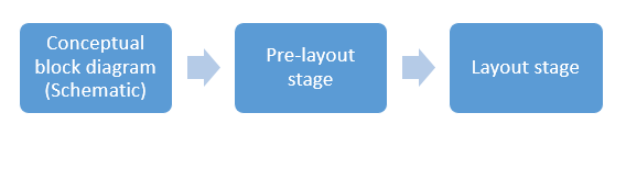
Drawing a schematic of a circuit is the initial stage in PCB design. CAD software is then used to convert this block diagram into schematic drawings. A schematic is made up of component symbols and the connections that connect them. These nets will become copper traces on the circuit board.
BOM is validated at the pre-layout stage of design for long lead and obsolete components.The manufacturing part numbers (MPNs) and vendor component numbers are checked during the validation process. Stack-up design is also done at this point.
Following the pre-layout stage is the layout stage. In the layout stage, the board parameters, board outline, component placement, routing, and production document generation are carried out.
Beat competitors to the market. Reduce Respins with our Zero-Defect Guarantee.
With Turnkey PRO, Sierra Circuits delivers full turnkey PCB assemblies guaranteed to work.
What is PCB layout?
The board layout stage includes setting up the design tool, board outline, import of netlist, component placement, routing, silkscreen cleanup, DRC check, and generation of documents for production (Gerbers, netlist, etc.). For more details see how to design a PCB layout.
Top design software used to design a circuit board layout
To become a successful PCB designer, it is essential to be proficient in electronic design automation (EDA) software, also known as electronic computer-aided design (ECAD) software, to produce schematics of the required circuit board. The produced design pattern must be in compliance with the IEEE electromagnetic compatibility (EMC) standards. This design is later put into production by a PCB manufacturer.
The prime factors to be considered while choosing a PCB design software are:
- User interface (UI)
- Features
- Large components libraries
Software programs establish a convenient approach in board design that can be easily transformed into a physical circuit board. Few of the popular PCB design software are:
- Altium designer
- Cadence Allegro Orcad
- KiCad
- Mentor Graphics pads and expedition
- Cadstar
- Zuken
- Eagle
- Solidworks PCB
Sierra Circuits’ engineers and technicians have the experience to bring your PCBs to life.
Start building your quote online now.
PCB layout rules to follow in your design
Plan your stack-up
Setting the stack-up and design rules is the first step in the layout stage. The stack-up design provided by the PCB manufacturer is used as a blueprint.
Set the design rules
Design rules ensure the board is easily manufacturable. They govern each and every area of the design.Some of the prominent PCB design rules are:
- Electrical design rules: Deal with electrical properties like impedance, voltage, and so on.
- Physical design rules: Related to factors such as trace width, via sizes, differential pairings, and so on.
- Spacing design rules: Associated with high-voltage power track spacing and clearance.

Controlled Impedance Design Guide
6 Chapters - 56 Pages - 60 Minute ReadWhat's Inside:
- Understanding why controlled impedance is necessary
- Stack-up design guidelines
- How to design for impedance
- Common mistakes to avoid
Download Now
Draw the board outline
The shape of the circuit board is referred to as the board outline and is essentially a closed contour. The board shape can be defined using a CAD tool.
Component placement
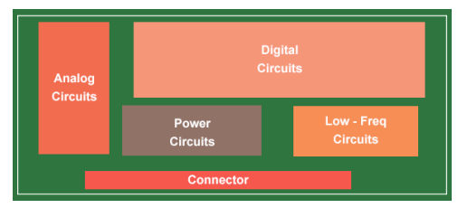
The initial stage in component placement is to divide the layout into sections based on the functionality of the circuit (analog, digital, high-speed, high-current, power supply, etc).
During component placement, SMT and through-hole components are mounted on the PCB at their fixed locations as per the design. Connectors and their accompanying components assembled initially. Essential components, such as the CPU, memory, and analog circuits, are then placed. The third stage is to connect the auxiliary components, such as crystals and decoupling, to the primary components.
Route the board nets
Routing is the process of connecting nodes by laying copper traces. This conductive path is defined by the placement of tracks, arcs, and vias on the copper layers to connect the two nodes.
The power/ground plane connections are made after the component routing is completed. The power plane is a layer of copper that connects the power supply. Similarly, the ground plane is a layer of copper that acts as ground.
Perform a design rule check (DRC)
Design rule check (DRC) is a process that verifies a design’s logical and physical integrity. Checks are performed against all of the enabled PCB design rules. This feature can also be enabled online, allowing you to perform the checks in parallel as you work through the design process. This step should be performed on every routed board to ensure that the minimum clearance rules have been followed and no violations have occurred.
Complete PCB fab/assembly notes
Board fab notes consist of the following design-related information:
- Class of the PCB (class 1/class 2/class 3)
- Number of layers
- Overall board thickness
- IPC standards to be followed
- Color of solder mask
- Color of silkscreen
- Layer-wise impedance details
- Cut-out details
- Stack-up details
- Drill-hole details (drill chart)
- Version number and date
Filling out all of the specific information on the fab notes is critical because it documents all of the important information about the PCB design for future reference.
Tips to design a circuit board layout:
- Choose the right PCB material. Fire retardancy, thickness, rigidity, flexibility, operating temperature, thermal resistance can all have an impact on the board.
- Ensure that your design files include all values and tolerances for trace width, copper thickness, board clearances, and drill hole. Learn more about PCB file formats to choose the right data set.
- All components and connectors must be at least 0.04” (40 mils) away from the board edge.
- Drill holes (plated and non plated) and copper traces should be placed at least 0.010”(10 mils) away from the board edge.
- Ensure that footprint pads match the components listed in the BOM.
- For markings and identifiers, use the silkscreen.
PCB layout is a basic but crucial aspect of design and manufacturing. Partnering with your contract manufacturer is the best method to assure a well-built and reliable circuit board.
Try our free Better DFM tool and save time and money.
Our automated platform will catch any PCB design error ahead of time and prevent on-holds and re-spins. Get started by uploading your Gerber files here.


