What are the manufacturing tolerances for PCBs?
Tolerance is the allowed diversion/variation from a specific dimension. It defines the acceptable variation between the maximum and minimum limits. For example, if an ideal part is to be 10mm with a tolerance of ± 1mm, any part that falls between 9 and 11 mm will be acceptable. PCB manufacturing tolerances with respect to material thickness, copper thickness, drilling, plating, and solder masks play an important role in the fabrication process. Maintaining these tolerances will ensure that your circuit boards are manufactured precisely.
Circuit board dimensional tolerances
Bow and twist tolerances
Bow and twist are flatness-based criteria that determine alignment problems in a circuit board.
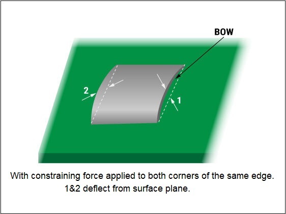
The bow is the deviation from the flatness of a circuit board. It is a cylindrical/spherical curve on a rectangular plane surface, as shown in the image above.
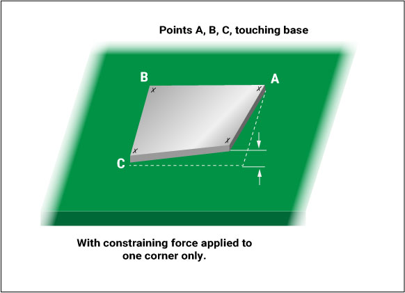
The twist is the deformation of a rectangular circuit board, causing one of the sheets’ corners to be off the plane containing the other three corners.
For non-rectangular boards, bow and twist can be measured by placing a rectangle over the PCB that is being tested. The imaginary rectangle’s dimensions should be the minimum that completely encloses the specimen.
Adhering to design for manufacturing guidelines can help you prevent bow and twist. To learn the DFM rules and best practices, download the DFM Handbook.

Design for Manufacturing Handbook
11 Chapters - 96 Pages - 90 Minute ReadWhat's Inside:
- Annular rings: avoid drill breakouts
- Vias: optimize your design
- Trace width and space: follow the best practices
- Solder mask and silkscreen: get the must-knows
Download Now
IPC 2422-1 and 2422-2 define the maximum bow and twist on circuit boards as:
| Features | Tolerance |
|---|---|
| Maximum bow and twist for boards with SMD | 0.75% |
| Maximum bow and twist for boards without SMD | 1.5% |
Circuit board thickness
The thickness primarily depends on factors such as copper thickness, materials used, number of layers, and the operating environment. The standard PCB thicknesses are 31 mils, 62 mils, 93 mils, and 125 mils.
Acceptable tolerances for board thickness
| Thickness | Tolerance |
|---|---|
| Boards with thickness 31 mils and above | ± 10% |
| Boards with thickness less than 31 mils | ± 0.003” |
Drilling tolerances
The drilling process is the basis for vias and layer interconnections. A design engineer must always look into the board manufacturers’ capabilities and tolerances before placing an order.
The table below summarizes the drilling tolerances followed at Sierra Circuits.
| Features | Tolerance |
|---|---|
| Drill diameter tolerance for PTH and NPTH drills | ±3 mils (0.003”) |
| Drill to copper | Minimum 8 mils (0.008”) |
| Tolerance in location/registration of the drilled hole | 1 mil (0.001") |
| Drill (hole) to drill (hole) | 6 mils (0.006") |
| Drill (hole) to board edge | 6 mils (0.006") |
| Annular ring tolerances | Will be specified by the designer |
| Laser hole location tolerances | 5 mils (0.005”) |
Routing tolerances
| Product features | Routed part size tolerance |
|---|---|
| Standard | 5 mils (0.005”) |
| Advanced | 3 mils (0.003”) |
| Micro | 3 mils (0.003”) |
| Product features | Laser routed part size tolerance ( can only be done with panels < .032” thick) |
|---|---|
| Standard | 2 mils (0.002”) |
| Advanced | 2 mils (0.002”) |
| Micro | 2 mils (0.002”) |
Controlled impedance tolerances
To achieve undistorted signal propagation through traces, a uniformly controlled impedance is a must to minimize signal reflections, hence distortion.
Controlled impedance tolerances at Sierra Circuits:
| Product features | Controlled impedance tolerance |
|---|---|
| Standard | 10% |
| Advanced | 5% |
| Micro | 5% |
Solder mask feature tolerances
| Product features | Solder mask feature tolerance |
|---|---|
| Standard | 1.5 mils (0.0015”) |
| Advanced | 1 mil (0.001”) |
| Micro | 1 mil (0.001”) |


