


Contents

On-demand webinar
How Good is My Shield? An Introduction to Transfer Impedance and Shielding Effectiveness
by Karen Burnham
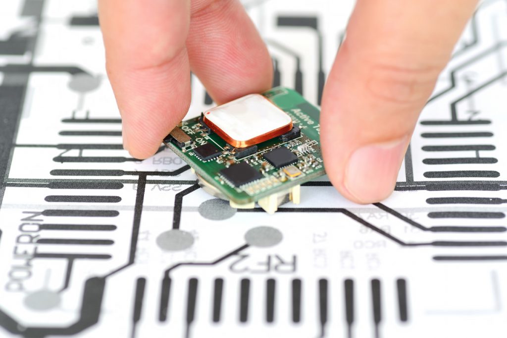
PCB is the backbone of all major electronic devices and is also responsible for making devices compact and efficient. A PCB manufacturer can achieve perfection only if the PCB designer provides a design data file or artwork, that completely describes the board specifications. So, let’s check out what are the different PCB design output data that a manufacturer requires.
Design files, otherwise known as artwork, are the prime communication bridge between fabricators and designers. A manufacturer can check the manufacturability of a PCB by running some advanced design for manufacturability (DFM) checks. For PCB manufacturing, the fabricator requires detailed Gerber or ODB++ files, or IPC-2581 imports/exports.
A PCB designer’s prime goal is to provide detailed documentation to ensure that the PCB manufacturer avoids any guesswork that could lead to undesirable outcomes in the board functionality. Hence, design data files are the bridge between manufacturers and designers.
PCB design output files for fabrication
Design files are the prime communication channels between fabricators and designers. Initially, Gerber files ruled the industry since its introduction in 1980. Towards the middle of the 90’s, the intelligent format ODB++ came into existence, soon followed by the open and neutral IPC-2581.
Here is a list of the different PCB design files you can send your manufacturer for fabrication:
- Gerber files
- IPC-2581
- IPC Netlist
- Drill files
- BOM (Bill of materials)
- Pick and Place files
- Fab drawing
- ODB++ files (OPTIONAL)
What is gerber?
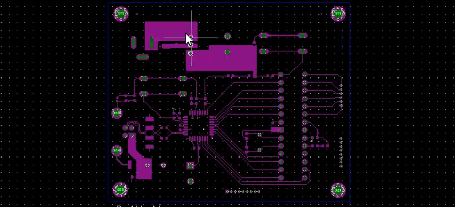
Once the layout design of a PCB board is completed and ready for the fabrication. The design is converted into a standard file format called Gerber files which can be used by the PCB manufacturers to manufacture PCBs.
The Gerber files are generated for each of the layers of the PCB. The PCB manufacturer produces as many as 30 or more layer files to define different aspects of manufacturing.
List of gerber file for manufacturing
- Aperture definitions
- TOP- Top layer – This defines the top copper layer, traces and pads
- SMT – Solder Mask Top – Defines the area where soldermask should appear on the top layer
- SPT – Solder Paste Top – Defines the solder paste applied to solder the components on the top layer
- BOT – Bottom layer
- SMB – Solder Mask Bottom
- SPB – Solder Paste Bottom
- SST – Silkscreen top – Defines the labels on the top layer of the components
- SSB – Silkscreen bottom – Defines the labels on the bottom layer of the components
- AST – Assembly top – Assembly instructions of the top layer
- ASB – Assembly Bottom – Assembly instructions of the bottom layer
- FAB – Gives details of drills, stack-up, cutouts, and fabrication instructions such as the class of fabrication (class 2, class 3).
Gerber file extensions
| Filename, Extension | Function |
|---|---|
| .brd | Mainboard project file |
| .rou | Board outline cutting path |
| .drl | Drill hole data |
| .GTS | Top solder mask |
| .GBS | Bottom solder mask |
| .GD1 | Drill drawing |
| .GG1 | Drill guide |
| .GTL | Top copper layer |
| .GBL | Bottom copper layer |
| .GTO | Top overlay |
| .GBO | Bottom overlay |
| GP1, GP2, GP3……. | Inner layers |
Gerber file formats
The number and types of files created by the gerber depend on the complexity of the board and the manufacturer’s specifications. The main type of gerber files is generated for each layer in the PCB design, while there are files to describe procedures across different layers. For example, files are generated for etching, silkscreen, drill files, etc.
The RS-274D and RS-274X (also known as Excellon), are the two most common types of output formats. And now there is the latest X2 version.
Also read: How to Export Gerber and Production Files in Altium Designer
Standard gerber (RS 274-D)
The first form of Gerber file representation was designed as numerical control (NC) format. The RS 274-D has provided simple plotting functionality such as truck drawing. It did not describe coordinates and drawing margins separately.
The RS 274-D standard gerber files are responsible for the success and popularity of the gerber file formats. The common extension used for these files is “.gbr” text. However, different design tools give different extensions.
Extended gerber (RS-274-X)
It uses human-readable ASCII commands that are combined to create a graphical 2D map. X-Gerber has introduced the use of metadata for the graphics description. This version incorporates all four components of the Gerber details in one file (configuration parameters, apertures, XY coordinates, draw and flash commands). This is associated with extensions of the “.gbr” and the “.gbx” formats.
Gerber X2
This is the latest version of Gerber files which supports additional data. Gerber X2 files can contain details such as the layer function, entity functions like pad types, trace positions regulated with impedance, and much more.
This file format supports extensions like “.top” and “.bot” and it is compatible with all types of modern CAM software.
Gerber files should be created with utmost precision. It is crucial to address and rectify the common issues associated with Gerber files, such as missing board outlines, unregistered layers, design files mismatch, etc.

What is ODB ++?
ODB++ is an intelligent format. A single ODB++ file or directory contains all the information required to define a PCB layer.
This file format offers a stable framework for the required data. An ODB++ file doesn’t ensure that the given data is sufficient to manufacture the design but it allows the designer to combine all the data and perform the required checks for manufacturability and reliability.
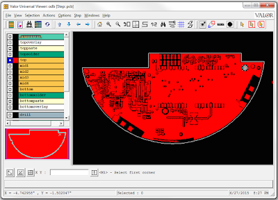
The ODB++ translator inputs an ODB++ archive or a compressed file (.tgz, .tar, .gz, .zip, or .tar) or a directory of files from a circuit layout program.
The ODB++ file is submitted to the manufacturer as a single file with .gzip extension. All required files are stored in this main file.
Why ODB++?
- The ODB++ hierarchy framework enables programmers and organizations to transfer more than just standard artwork and drill data.
- It can allow additional data in a single file. For example, it can consist of material stack-up, bill of materials, component placement, as well as dimension and fabrication data.
- ODB++ can be accessed via most PCB design programs (Expedition, PADS, Allegro), making it almost a universal format.
- It allows simple and effective production of the component without the complexity.
- This intelligent file is supported by all major vendors of CAD, CAM, and DFM tools.
What’s the difference between ODB++ and gerber files?
Gerber RS274X is the most widely used format for PCB design. It is a single PCB file that includes all the layer data, pad shape, and drawings providing an accurate design.
But a Gerber cannot define the layer stack-up and the drill files cannot be included, while ODB++ can include a huge amount of data.
ODB++ is a more intelligent file format since a single file could include a large amount of data. Most of the fabricators now prefer ODB++ because it helps reduce human errors. Using ODB++, a PCB manufacturer could remove the necessity of working with a lot of low-level files.
What is IPC-2581?

IPC-2581 is a universal PCB assembly and manufacturing standard for data definition and transition methodology. IPC-2581 can include a large number of files within a single XML file.
Also recognized as “Standard Specifications for Manufacturing Description Data and Transfer Methodology for Printed Board Assembly Products,” is the IPC-2581 standard.
IPC 2581 includes the following data:
- Copper structures per layer
- Order of build-up
- Layer stack information
- Netlist in-circuit testing
- Material information
- Drill data
- Test points
- Assembly notes
- Bill of materials for purchase
Drill files
PCB drilling is the basis for the vias and the connectivity between various layers. Drilling is the most expensive, irreversible, and time-consuming process in the manufacturing process of PCBs. A small malposition may require refabrication of the whole board from scratch.
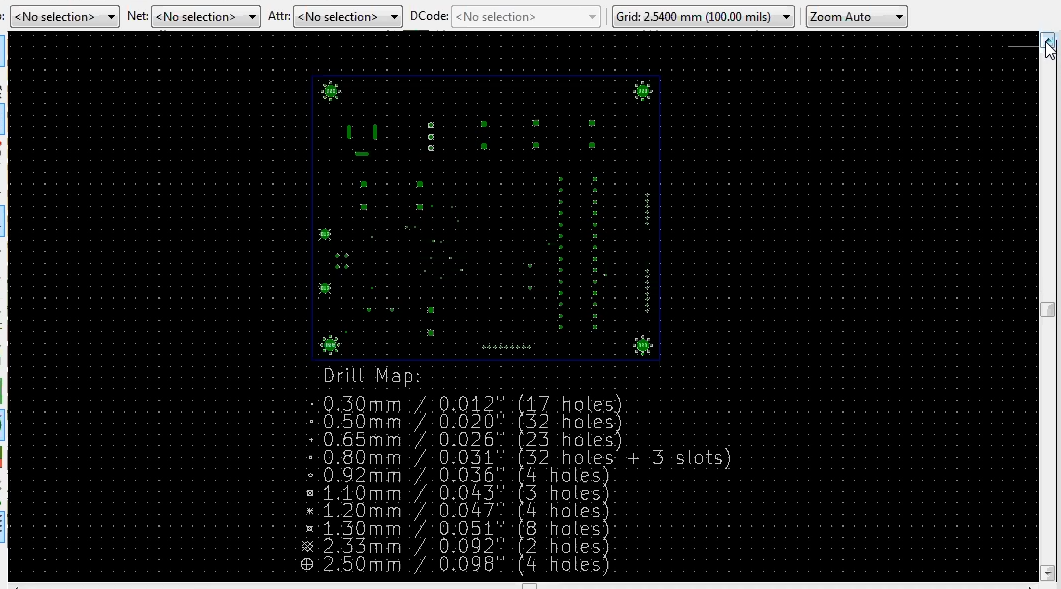
A drill file is a secondary file sent to the manufacturer with the Gerber file. The drill file refers to the position, size, and the number of holes in the desired PCB. The NC drill file can be used to correctly determine where all the drill holes are located on your board and the size they require. The number of files created for the drill varies depending on the complexity of PCB wiring. Drills can be of different types: through-holes, blind vias, and buried vias.
Types of drill holes
There are two types of holes to be drilled in the PCB, plated and non-plated holes. Non-plated holes are normally used as mounting holes for the PCB and as positions holes for connectors. If the PCB has to be electrically isolated from the enclosure non-plated mounting holes are used. If the PCB has to be grounded to the enclosure plated mounting holes are used. All interconnect vias which connect different layers are plated. If a board design has both plated and non-plated holes, you can merge the drill details in one NC drill file for both types of holes or have different NC drill files created by the PCB design tool.
Usually, two separate files are created for plated and non-plated holes. This is because the plated through holes are drilled before the plating process happens, whereas, the non-plated holes are drilled after the plating process.
Drill file extensions
The regular, plated drill file uses ‘.drl’ file extension and non-plated hole drill files have ‘np’ in the file name; eg: ‘np.drl’.
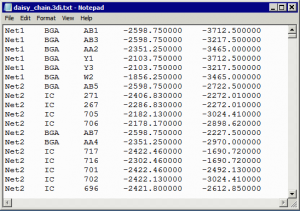
What is a PCB netlist?
The netlist (formatted as IPC-356) is a list of networks that determine a bare circuit board’s conductivity interconnection scheme. In general, the netlist is an ASCII text file that includes the PCB CAM system instructions such as net names, pins, and XY coordinates of the start and endpoint for each net or node.
Why do we use a netlist?
Gerber 274x does not support the netlist. In certain instances, Gerber files exported from your PCB CAD software can contain an unnoticed error, because there is no way to verify whether the files are in accordance with your design intent. You can prevent this by loading your manufacturing data kit with an IPC-356 format netlist file. The IPC netlist aims to find defects in the pre-production process.
The customer’s CAD netlist will be compared by the fabricator with the list derived from the Gerber data provided by the customer. The customer will be notified about any errors during the analysis.
What do we do with the PCB netlist?
- We check if the designer’s netlist is the same as the manufacturer’s netlist created on the basis of their graphic data.
- We check the netlist data each time we edit the board so it doesn’t cause any netlist violation.
- Fabricators use the customer-supplied netlist during the electrical validation of the PCB.
Bill of Materials (BOM)
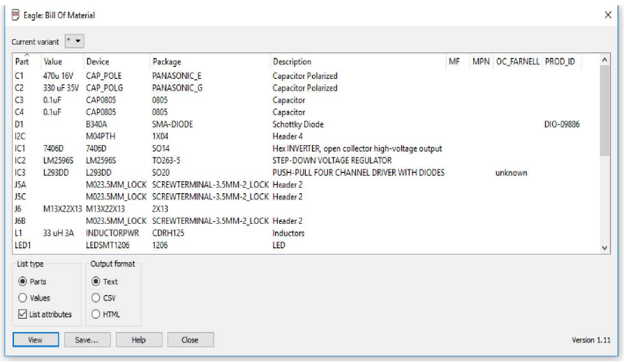
BOM or Bill Of Material contains the list of all components and its specification required for fabrication of the design. Designers can generate customized BOM from their designing software, that lists all of the footprints of the components in an Excel spreadsheet. These BOMs are used as a reference for the fabricators to assemble the components in the correct order by referring to the footprints and designator.
Designers can many types of information to their BOM, but a set of information that are required in BOM is listed below:
- Reference designator
- Part description
- Do not insert (DNI) yes or no
- Quantity
- Manufacturer part number (MPN)
- Vendor part number (VPN)
- Footprint of the component
- Comments.
Pick and place files
PCB manufacturers use Pick and Place machines during the assembly process to pick the right component and place it at the desired position. These machines need proper data to do so. Pick and Place files hold such data in ASCII text format which can be generated using any designing software after the design completion.
The main purpose of a pick and place data is to hold information about the position and orientation of all surface mount devices on a circuit board design. So Pick and Place files contain data such as:
- Reference designators
- XY locations of the component in the board
- Orientation of the component in degree (45° 90°.. etc)
- Component packages – Part number, Part value, etc.
- Placement on either the top or bottom side of the board.
FAB drawings
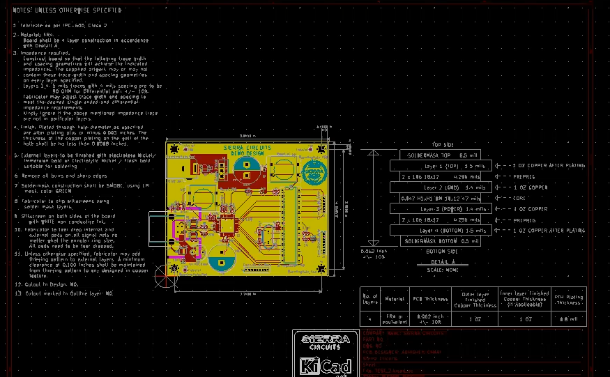
The Fab drawings give the manufacturing details of the PCB, this includes board dimensions, drill details, class of fabrication (class 2, class 3), and stack-up details. Fabrication drawings are sent in PDF format to manufacturers and all designing tools support the function that exports PDF-formatted FAB drawings.
Designers can mention all the required details in the fab drawing that are important for PCB fabrication. But consider including these data:
- Dimensions of the board:
Mention the Length, width, thickness of the board
- The board outline:
Board outline must be drawn on the ‘board outline’ layer. Additional images of outlines should be added for denser boards with a lot of buried vias. This can ensure a detailed view of the stacked vias.
- Drill chart:
Mention the different types of drills used, such as laser holes, micro via, via on pad, plugged via, and blind/buried via. Drill chart also contains the drill size, which layers are to be drilled
-
-
-
- Holes are drilled on to a PCB for various functions. Standard drill bit sizes are specified in ANSI standard B19.11M. There are a number of techniques to reduce the size of the hole in order to reduce the size of the entire board. Mostly, the hole dimension mentioned in the files will be actual drill size, not the finished hole size.
-
-
- Stack-up drawing:
Designers can draw a stack-up describing details such as the thickness of each layer, the thickness of the top and bottom solder mask.
-
-
-
- Finished PCB thickness: Final thickness is the combined thickness of all layers, including core and prepreg thickness. Normally the finished PCB thickness is 62 mils.
- Core thickness: Core is one of the main parts of the PCB layers. There are different ranges of core thickness that are plated with copper on either side, top and bottom.
- Prepreg thickness: Prepreg is used to join two different cores or a copper foil in a stack-up. The prepreg thickness depends on its adjacent layers, like the signal layer or plane layer.
- Copper thickness for PTHs and vias: Copper is plated inside the component holes drilled in the PCB. The thickness of the plating is usually 20 to 100 microinches, depending on the capabilities of the fabricator.
- Copper cladding thickness: The thickness of copper-clad is an important parameter that will be requested by the manufacturer. The thickness depends on the strength of current passing through traces and the width of traces.
-
-
- Copper trace and etching tolerance:
While the process of etching the copper near the etch resist begins to be removed under the mask. This is called etch-back or undercutting. The width tolerance for etch-back is defined by IPC-2221A, which varies from 4 mils to 0.6 mils for 1 1⁄2 oz copper, depending on the degree of reducibility and plating.
- Class of fabrication (class 2, class 3)
- Color of the soldermask and silkscreen
- Highlight the impedance traces on the PCB
The PCB manufacturer expects different data from the designer. These can be in gerber formats, gerber X2 format, ODB++.

Design for Manufacturing Handbook
11 Chapters - 96 Pages - 90 Minute ReadWhat's Inside:
- Annular rings: avoid drill breakouts
- Vias: optimize your design
- Trace width and space: follow the best practices
- Solder mask and silkscreen: get the must-knows
Download Now


