Contents

On-demand webinar
How Good is My Shield? An Introduction to Transfer Impedance and Shielding Effectiveness
by Karen Burnham
In circuit board manufacturing, the process of implementing the PCB surface finish is critical in enhancing the reliability and shelf life of the PCBA. We will cover the various types of surface finishes that the printed circuit boards are given to enhance good inter-metallic bonding and the shelf-life of the assembly.
Current-day PCB assemblies consist mostly of SMT components, where pad flatness is a significant consideration. Such PCBAs use electroless nickel and immersion gold surface finish. Based on the customer applications, there are other surface finishes that are also available, like soft gold, sterling silver, and OSP finishes. Sierra Circuits can process various types of surface finishes according to customers’ needs, such as hot air solder leveling (HASL), hot air solder leveling lead-free (HASL lead-free), electroless nickel immersion gold (ENIG), and electroless nickel electroless palladium immersion gold (ENEPIG). These different types of surface finishes enhance the shelf life of the board, with each surface finish having a different shelf life.
The most commonly used surface finishes are hot air solder leveling (HASL) with tin/lead alloy. Due to RoHS guideline policies, the boards that are RoHS compliant should not contain lead. Hence, in the same HASL process, we are using only tin and its associated alloys for lead-free requirements.
What is a surface finish in PCB?
A PCB surface finish is an intermetallic joint between the bare copper of the solderable area of the printed circuit board and the components.
Circuit boards have a base copper surface that is susceptible to oxidation if left without a protective coating, hence the requirement of the surface finish. It is also responsible for preparing the PCB surface for soldering components onto the board during assembly and enhancing the shelf life of the board.
Read the PCB surface to learn about the surface layers of a PCB.
Significance of a PCB surface finish
It impacts various features such as:
- The quality of the inter-metallic joint
- The process yield
- Rework for production batches, along with the scrap rate
- Testing ability
- Cost of the manufacturing process
- The rate at which the board will fail while being used for its intended application
What are the types of PCB surface finishes?
They can be broadly classified into metallic and organic.
Metallic surface finishes
These surface finishes use metallic layers as a protective coating for the PCB copper layer.
Also read, what is conformal coating?
What is HASL PCB finish? (Hot air solder leveling)
HASL is a conventional surface finish applied to circuit boards. The circuit board is generally dipped into a molten solder bath to cover all exposed copper surfaces with solder. Surplus solder is separated by passing the board between hot-air knives. The solder is a tin-lead mixture in this case.
Since the introduction of the RoHS (Restriction of Hazardous Substances) requirement, lead-free HASL has been widely used.
Advantages
- Provides superior wetting during component soldering
- Prevents copper corrosion
- Permits a larger processing window
- Widely used for boards without RoHS restrictions
Disadvantages
- Thickness varies between large and small pads
- Unsuitable for < 20 mil pitch BGA and SMD
- Bridging on fine pitch
- Not preferable for High-density interface (HDI) products
Lead-free HASL
This is a variation of HASL where lead-free alloys are used, such as Sn/Ag/Cu (SAC), Sn/Cu/Co, Sn/Cu/Ni/Ge
Advantages
- Potential delamination issues can be spotted by exposing the PCB to temperatures of 260°C
- Widely available
- Eco-friendly
- More durable compared to other finishes
- Comparatively more re-workable
- It is more affordable
Disadvantages
- May generate thermal shock
- It may result in uneven surfaces
- Not preferable for fine-pitching
- It may bridge solders
What is immersion gold plating?
ENIG, or electroless nickel immersion gold, includes electroless nickel plating covered with a thin coating of immersion gold, shielding the copper from oxidation.
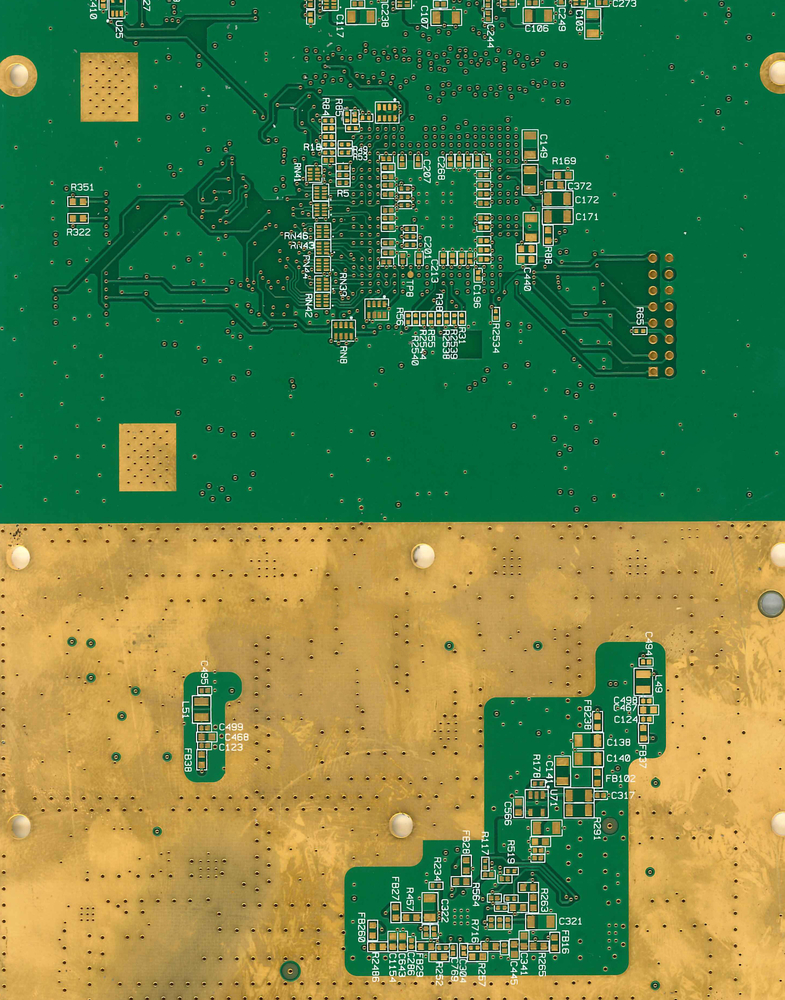
Advantages of ENIG
- This is ideal for flip chips and BGAs when compared to other surface finishes
- Ideal for flat surfaces since the layers of nickel and gold are thin and even
- No lead making it RoHS-compliant
- Preferable for PTH
- Comes with a long shelf-life
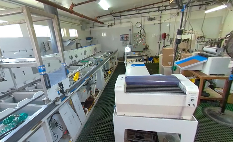
Surface finish station at the Sierra Circuits manufacturing facility
Disadvantages of ENIG
- Often leads to a “black pad”. This is where there is a buildup of phosphorus between the nickel and gold layers. This might result in fractures and faulty board connections
- Not ideal for reworking
Electroless nickel deposition is an auto-catalytic process where nickel is deposited on the palladium-catalyzed copper surface. To get a consistent coating, the reducing agent-containing nickel ions must be refilled in order to offer proper concentration and temperature. While implementing the immersion gold step, the gold will adhere to the nickel-plated areas, protecting the nickel until the soldering process.
Due to its high reliability, ENIG finds its dominant application in castellated circuit boards, SMT, lead-free soldering, and BGA packages.
What is ENEPIG plating?
ENEPIG, or electroless nickel electroless palladium immersion gold, is a variation of ENIG. Here, a coating of palladium is done as a protective layer to stop the oxidation of nickel and to stop diffusion to the copper layer. Even though the cost of ENIG and ENEPIG is higher than other surface finishes, it provides excellent solderability for PCBs.
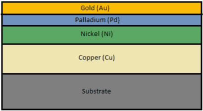
What are the advantages of the ENEPIG finish?
- It is applicable for a wide range of boards, earning the name ‘universal finish’, It can be used for varied surface packages and highly advanced boards.
- Easy to process
- Lead-free, hence RoHS compliant
- Great for multiple reflow cycles
- Highly compatible with Sn-Ag-Cu solders
- Long shelf-life
Disadvantages of ENEPIG
- Frequently results in the occurrence of black pad
- Decreases the reliability of solder joints
- The thickness of the palladium layer does not support solderability performance
- Longer duration is required to wet when compared with other surface finishes
- The efficiency is affected by plating conditions
- Higher cost compared to other surface finishes
ENEPIG plating may not be the best choice for advanced boards with tight spacing. EPIG surface finish eliminates the electroless nickel layer, significantly reducing material build-up on traces and allowing for finer features and reduced clearances.
What is hard gold?
Hard gold includes a layer of gold that is plated over a nickel coat. Hard gold is a gold alloy consisting of nickel, cobalt, or iron and is best suited for components with a higher probability of wear and tear, such as edge connectors, interconnected carrier boards, contacts, and keypads. The thickness of this finish will vary according to the application where it is used. Hard gold is not generally applied to solderable areas because of its high cost and its relatively poor solderability.
Advantages:
- It is a hard and durable surface finish that is suitable for high degrees of wear
- Lead-free finish, making it RoHS-compliant
- Long shelf life
Disadvantages:
- More expensive
- It involves more processing and is labor-intensive
- The finish does not fully cover the sidewalls of the trace, except in the finger areas
- The etching undercut defect can lead to slivering or flaking
What are PCB gold fingers?
The gold-plated columns that can be seen along the connecting edge of PCBs are also called PCB gold fingers. The function of gold fingers is to connect a secondary PCB to the computer motherboard. Gold fingers make it possible for different circuit boards to communicate with one another. Signal transmission from the power source to the device or equipment is made possible by PCB gold fingers. PCB gold fingers are used in various devices such as smartphones and smartwatches. The gold coating is used for the connecting edges due to its superior conductivity.
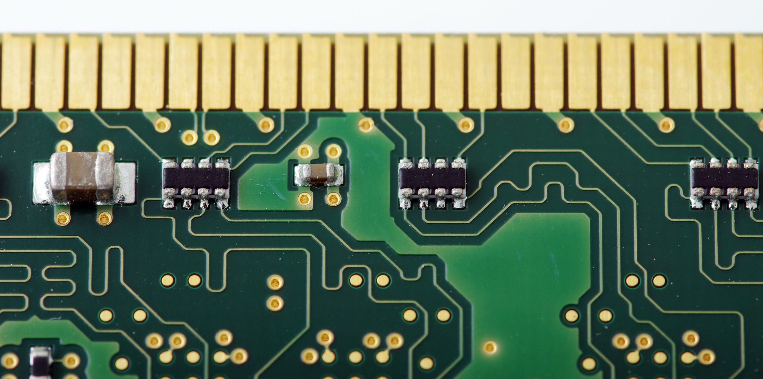
Hard gold finish processes are used to make PCB gold fingers.
The standards involved in the plating process help to ensure a perfect fit between the gold fingers on each circuit board with the corresponding slots on a given motherboard. There is a battery of tests conducted to check for layer thickness and smoothness of the gold plating.
Immersion silver (ImAg)
Immersion silver consists of a lead-free layer of silver plated onto a PCB to protect copper traces from corrosion. Silver surface finishes can be applied to copper traces with an electroless immersion reaction, displacing the copper layer.
Advantages of immersion silver
- Suitable for fine pitch
- Long shelf-life of around 12 months
- Stable compared to other surface finishes
- Ideal for planarity requirements
- It is affordable and cost-effective
Disadvantages of immersion silver
- It may lead to silver whiskering, which is the formation of hair-like metal projections on the board surface
- Unsuitable for compliant-pin interaction as it is susceptible to fracture
- Not ideal for micro vias with aspect ratios of 1:1
Immersion tin (ImSn)
Immersion tin includes a thin layer of tin deposited on the copper layer of a PCB. This is a lead-free and hence RoHS-compliant surface finish, which is a great choice for small geometries and components. It is suitable for flat surface requirements and fine-pitch components.
Advantages
- This allows excellent planarity or flatness, which is suitable for fine pitch or BGA components
- Suitable for press-fit
- Lead-free finish for immersion tin is available at a mid-range cost
- Immersion Tin has a mid-range cost for a lead-free finish
- Retains good solderability after multiple thermal cycles
Disadvantages
- Susceptible to handling.
- Short shelf-life, tin whiskering defect can occur after 6 months
- Unsuitable for use with peelable masks
- Unsuitable for contact switches.
- Special equipment setup required (such as soft probe landing) for electrical test
Organic surface finish
This type of surface finish uses organic compounds (compounds that include Carbon) to form a protective coating over the copper layer on the PCB.
OSP (organic solderability preservative)
OSP is a water-based organic surface finish used for copper pads. It selectively bonds to the copper and protects the pad prior to soldering.
Advantages
- It is lead-free
- Works well for flat surfaces
- Involves a simple process
- Easy to rework
Disadvantages
- Unsuitable for PTH
- Handling this finish is a challenge
- Has a short shelf life
Carbon ink surface finish
Here, the copper pad on the PCB is coated with a protective layer of carbon ink. This surface finish method can be used in RF Shielding, keypads, keyboards, remote controllers, automotive vehicles, and welding equipment. The key factor in carbon ink PCB production is to control the printing, baking, and resistance control. The carbon ink can be printed onto almost any circuit board.
Also read Case Study: PCBs for Automotive Sensors.
Advantages
- Serves as a cost-effective alternative to the hard gold finish
- More robust compared to other types of finishes
Disadvantages
- Extra care and different cleaning steps are required
How to choose a PCB surface finish?
The final surface finish for a board is a critical factor that will decide the long-term reliability of the said PCB. You will need to consider the environment in which the circuit board will be used, such as a harsh environment with extreme temperatures. Also required will be the applications for which they will be used and the hours of operation.
Surface finish comparison chart
The table below is meant to help you understand the types of surface finishes used in reflow, aluminum wire bond, and gold wire bond assembly applications. It also details the relative cost of each finish compared to other types.
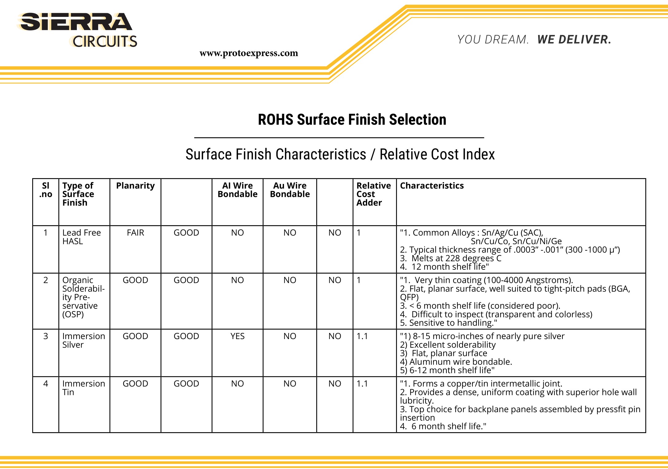
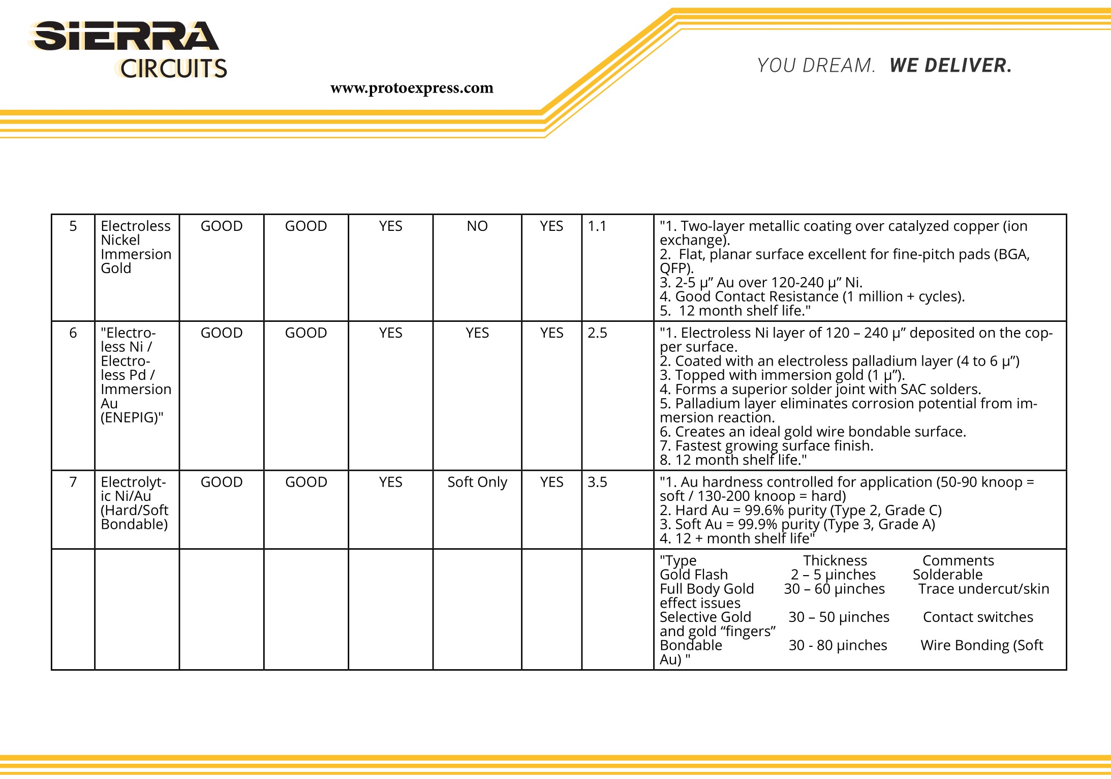
Some important factors to consider while selecting the surface finish:
- The environment in which the board will be used
- Aesthetics of the board – if the board needs a silver finish
- Shock and drop issue in the product. For example, when a smartphone is dropped, there is a risk of component fracture in the PCB. In such a scenario you would not use ENIG, which will have a tin-nickel bond, instead, you will need to use a tin-copper bond. However, you can use ENIG on medical devices.
- Corrosion is also a factor. For example, a silver finish is prone to creep corrosion
- The reliability requirement for the board is also an important parameter. If the product fails, what will be the cost of failure?
- Presence of fine pitch devices/components
- The flatness of the SMT pads for BGA applications
PCB manufacturing is a complex process to ensure the board manufactured meets the customer’s quality requirements. Guaranteeing the manufactured circuit board has the right surface finish according to the application will secure good PCB shelf-life and reliability.
Do you have any questions about the PCB surface finish? Let us know in the comments section, and we’ll get back to you!
Design for Manufacturing Handbook
11 Chapters - 96 Pages - 90 Minute ReadWhat's Inside:
- Annular rings: avoid drill breakouts
- Vias: optimize your design
- Trace width and space: follow the best practices
- Solder mask and silkscreen: get the must-knows
Download Now


