


Contents
Electronic devices are shrinking in size and increasing in complexity due to improvements in VLSI technology. The need for more interfacing input/output (I/O) leads and smaller device sizes has increased, and this need can be met with the BGA (Ball Grid Array) package.
BGA ICs having 4 pins or more than 500 IOs are commonly available. Such BGA ICs have a smaller form factor and help decrease the size of circuits. This enables the design and manufacture of compact products.
BGA devices are used extensively in modern products such as mobiles, PCs, and various communication devices.
In this article, you will learn the fundamentals of BGA and PoP packages, their key features and types, soldering and inspection methods, and important design considerations that help engineers successfully integrate BGAs into modern PCB designs.
Highlights:
- BGA packages enable high I/O density in a smaller board footprint
- Shorter interconnects improve signal integrity and high-speed performance
- Widely used in compact electronics such as mobile devices, PCs, and communication systems
- Require precise footprint design and controlled soldering processes
- Inspection and rework demand specialized techniques such as X-ray analysis
What is a BGA?
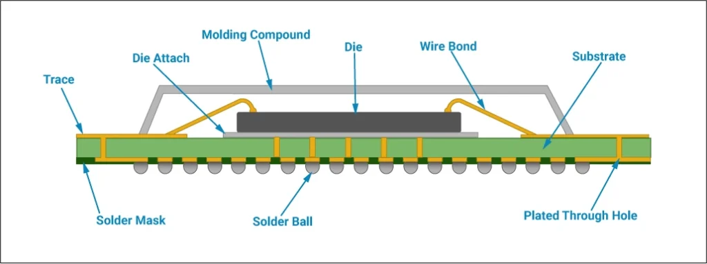
A ball grid array integrated circuit is a surface-mount device (SMD) component that possesses no leads. This SMD package employs an array of metal spheres that are made of solder, called the solder balls, for connections to the printed circuit board. These solder balls are affixed to a laminated substrate at the bottom of the package.


Figures 1 and 2 display two examples of how BGA devices are constructed. Figure 1 shows how the BGA die/chip is mounted on the substrate and connected to the substrate by wire bonding technology. Figure 2 displays how the BGA die is connected to the substrate using flip-chip technology.
The BGA die connections are routed to the solder balls using metal traces on the substrate. BGA packages can provide more I/O connections compared to dual-in-line or flat packages.
The connections from the die to the balls in BGA ICs are, on average, shorter than perimeter-only type connections such as DIP ICs. Thus, leading to better performance at high speeds.
Download our HDI PCB Design Guide to learn how to design a high-density board.

HDI PCB Design Guide
5 Chapters - 52 Pages - 60 Minute ReadWhat's Inside:
- Planning your stack-up and microvia structure
- Choosing the right materials
- Signal integrity and controlled impedance in HDI
- Manufacturing considerations for higher yields
Download Now
What is a BGA PoP?
It is a semiconductor packaging technique in which multiple integrated circuit packages are stacked vertically, with solder balls providing both mechanical support and electrical interconnection between the packages and the PCB. Package on package (PoP) allows packages to be assembled together, such as a logic device or memory package stacked with a processor.
This greatly reduces the requirement for PCB area and minimizes signal integrity issues on the board. Finally, it helps to improve overall board performance at an additional cost.


Advantages:
- Reducing component size
- Minimizing overall cost
- Reducing board complexity
Of all the packages, the BGA is the most popular package used in high I/O devices in the industry.

To select the right board type for microchips, see how to choose the right PCBs for IC integration.
7 important features of ball grid array packages
Critical properties of BGAs are:
- High lead count
- No leads to bend
- High interconnection density
- Occupies less space on the board
- Low inductance
- Self-centering during the reflow process, which reduces placement problems during surface mount soldering
- Lower thermal resistance between the package and the PCB. This allows heat generated by the integrated circuit inside the package to flow more easily to the PCB, preventing the chip from overheating.
Learn how to breakout a .4mm BGA.
4 commonly used BGA package types
The most popular BGA packages are:
- Plastic over-molded BGAs (PBGAs) (Ball pitch 1.0mm, 1.27mm) are an alternative form of the standard BGA. These BGAs incorporate a plastic-coated body, a glass-mixture laminated substrate, and etched copper traces. PBGAs feature improved temperature stability and preformed solder balls
- High thermal metal top BGAs with low profile (HLPBGAs)
- Flex Tape BGAs (TBGAs)
- High thermal BGAs (H-PBGAs)
One important point PCB designers need to follow is to have the correct footprint pattern for the BGA device. This is because once the BGA is soldered, it is very difficult to find any shorting or soldering problems. Also, investigating and fixing such problems involves a high cost.
Hence, adequate care must be taken to design the PCB footprint pad. The footprint pattern design and routing pattern strategy are dependent on the pitch of the BGA device pins/balls. The table given below lists the different pitches available in BGA packages.
| BGA pin count | Ball pitch (mm) | Signal layer count | |
|---|---|---|---|
| 2-trace | 1-trace | ||
| 256 | 1.0 | 2 | 3 |
| 324 | 0.8 | 2 | 3 |
| 484 | 0.8 | 3 | 4 |
| 484 | 1.0 | 2 | 4 |
| 625 | 0.8 | 3 | 4 |
| 676 | 1.0 | 3 | 5 |
| 784 | 0.8 | 4 | 5 |
| 900 | 1.0 | 3 | 5 |
| 1156 | 1.0 | 3 | 6 |
| 1517 | 1.0 | 4 | 7 |
| 1760 | 1.0 | 4 | 8 |
| 1924 | 1.0 | 4 | 8 |
| 2577 | 1.0 | 5 | 9 |
| 2892 | 1.0 | 5 | 10 |
How is a BGA soldered to a PCB?
In the PCB assembly process, the BGA is soldered onto the circuit board by the solder reflow process, using a reflow oven. During this process, the solder balls melt in the reflow oven.
Your assembly house should stick to these considerations to ensure an error-free assembly:
- Sufficient heat must be applied to ensure that all the balls in the grid melt sufficiently for every BGA solder joint to establish a strong bond.
- The surface tension of the molten balls helps hold the package in place on the PCB until the solder cools and solidifies. An optimum temperature-controlled BGA soldering process is necessary for solid solder joints and also to prevent solder balls from short-circuiting each other.
- The composition of the solder alloy and soldering temperature are precisely chosen so that the solder doesn’t completely melt but stays semi-liquid, allowing each ball to stay separate from its neighbors.
Learn how to breakout a .5mm BGA.
How are BGA solder joints inspected?
BGA solder joints are inspected using X-ray inspection to evaluate the hidden solder connections beneath the component.
Optical techniques cannot be used to inspect BGAs since the solder joints are hidden from sight beneath the BGA components. Also, electrical tests aren’t very reliable since the tests reveal the electrical conductivity of the BGA at that particular instant.
This test doesn’t predict if the solder will last long enough. The solder joint may, in fact, fail over a period of time.
X-ray inspection for BGA
The BGA solder joint bonds are inspected using X-rays. The X-ray inspection helps to look through the device’s solder joints underneath the components. Due to this ability, the automated X-ray Inspection (AXI) technology is widely used for BGA inspection.
There are many types of inspection tests available, such as manual, AOI, ICT, functional tests, etc. Refer to our post on the PCB assembly inspection report format to get a thorough understanding of all these tests.
Sierra Circuits fabricates and assembles high-quality circuit boards in the United States. Visit our PCB manufacturing capabilities to learn more.
How are faulty BGAs removed?
Defective packages are detached from the board by melting the solder joint. This is done by locally heating the BGA component until the solder joint melts underneath it.
In the rework process, the component is heated in a dedicated rework station. This consists of an infrared heater, a thermocouple that monitors the temperature, and a vacuum device to raise the package. You must ensure, with great precaution, that only the faulty BGA component is heated without damaging the neighboring components on the board.
Learn how HDI boards can be more economical
BGA components are well established in the electronics industry for their numerous advantages, in both mass production and prototyping. As the component count increases on the PCB, the routability and component placement become complex. The complexity of component density can be better managed with BGA packages.
BGA devices are increasingly used in the industry and have the advantage of having higher IO counts in less space, and therefore are suitable for complex and compact electronics design.
Have queries regarding designing high-speed boards? Post them on our community, SierraConnect. Our design experts will answer them.

About Rahul Shashikanth : Rahul Shashikanth is an electronics and communication engineer with over 8 years of experience in publishing technical articles on PCB design, manufacturing, and assembly. He is currently the content marketing manager at Sierra Circuits.


Start the discussion at sierraconnect.protoexpress.com