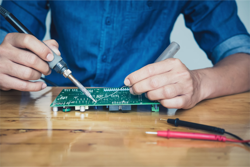
What is manual soldering?
Manual soldering is a traditional method of soldering leaded components to a PCB. It is generally used for small production runs, laboratory assembly work, rework/repair, and addition of extra components on a machine soldered assembly.
Manual soldering design considerations
In any electronic product, the points in the circuit which require manual soldering should be identified and instructions should be included in the assembly drawing. This type of soldering is used when a board design includes some parts that are not suitable for either reflow or wave soldering. The design considerations are as follows:
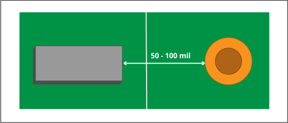
Part-to-part spacing
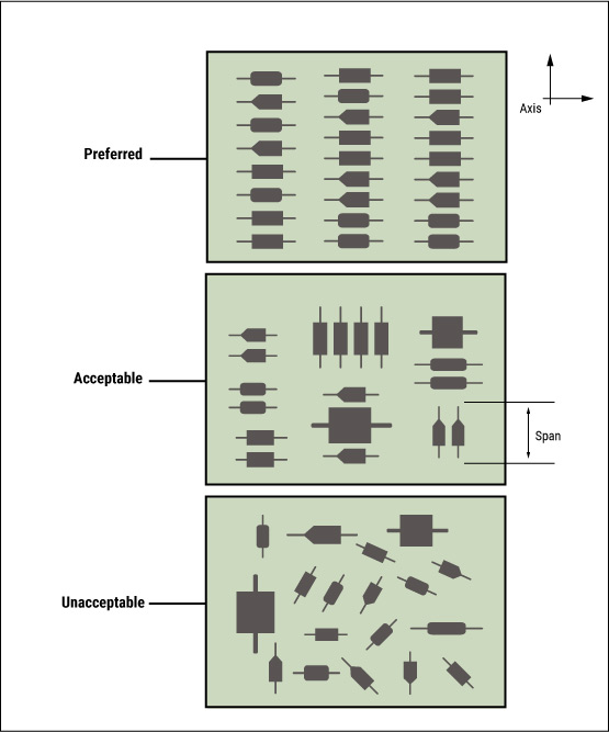
Manually soldered components should be placed further away from other components to avoid solder bridging. Typically, 50 to 100 mil pad-to-pad spacing should be maintained.
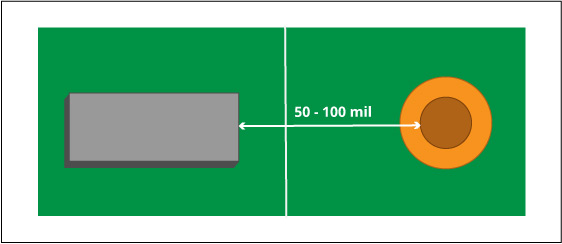
Part-to-hole spacing
Part-to-hole spacing applies to both through-hole components and vias; it stipulates the minimum spacing needed between a component pad or body and a hole. This spacing is divided into two categories:
1. Part-to-hole wall: It is the spacing measured from the edge of the hole to the edge of a pad. Typically, 50 to 100 mil.
2. Part-to-annular ring: It is the spacing measured from the edge of the hole’s annular ring to the edge of a pad. Typically, 50 to 100 mil.
Soldering Flux eBook
13 Chapters - 24 Pages - 40 Minute ReadWhat's Inside:
- Why flux is needed
- The ingredients of flux and what they do
- Soldering flux categories
- How to read a flux manufacturer’s technical data
- The best flux for various applications
Download Now
Surface finish
The selection of the surface finish is crucial for ensuring reliable soldering. It influences the process yield, amount of rework, scrap rate, and the cost.

The following are some of the most popular surface finishes:
Surface finishes Manual soldering challenges
ENEPIG - electroless nickel electroless palladium immersion gold Slightly less solder spread, incomplete pad coverage
ENIG - electroless nickel immersion gold Slightly less solder spread, incomplete pad coverage
Immersion silver (ImAg) None
Immersion tin (ImSn) None
Organic solderability preservative (OSP) Incomplete pad coverage, PTH hole fill, copper dissolution
HASL Copper dissolution
Pb-free HASL Copper dissolution
Hard gold None
Component selection and placement
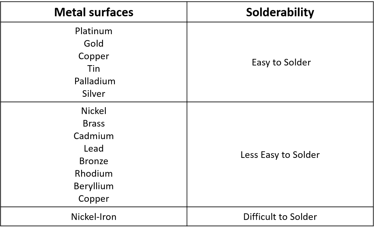
Component selection and placement is very important in the manual soldering process. The features that influence the process include the size, type, and plating of the component leads.
The metal solderability chart shows the solderability of different lead finishes.
Plated-through hole fill
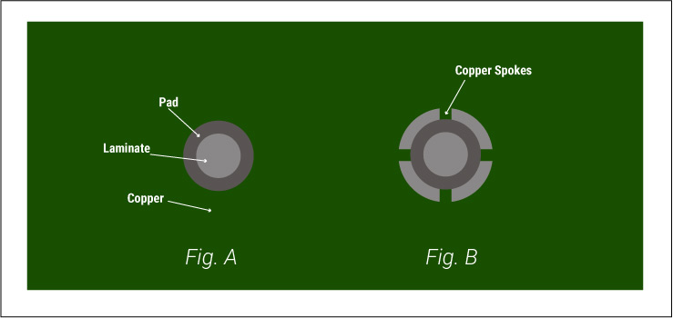
Achieving 100% PTH fill is difficult with manual soldering to an OSP surface finish because the OSP is affected with each thermal cycle. As a result, the underlying copper oxidizes, reducing solderability. Thus it requires the use of very active fluxes. A typical product undergoes two or more thermal cycles, such as bake, reflow, and wave, by the time manual soldering happens.
Designers should consider hole diameter, hole aspect ratio, and adequate thermal relief for large copper planes. It is necessary to utilize thermal relief on all copper planes since this reduces the thermal transfer rate between the PTH and the copper plane. This allows for easier solder joint formation during soldering and induces better hole fill.