What are the PCB mechanical processes used in fabrication?
PCB mechanical processes for fabrication typically involve drilling, scoring, grooving, etc. The profiling information is usually included in the Gerber file. It gives all the required instructions to the CNC machine or router to perform certain operations.
After testing, the boards are brought into the milling room to separate them from the large production panel. The operator loads one or more circuit boards onto the CNC machine and selects the appropriate program.
Beat competitors to the market. Reduce Respins with our Zero-Defect Guarantee.
With Turnkey PRO, Sierra Circuits delivers full turnkey PCB assemblies guaranteed to work.
Procedures involved in circuit board fabrication
Three outlining mechanical processes associated with manufacturing are V-scoring, milling, and back-drilling. Let’s review these operations in brief.
What is V-scoring?
V-scoring involves cutting straight tapered lines from both sides of the board. It is implemented for medium to large volume production with panels that only require straight line cuts. The panel can be assembled as one large board with minimal space between units.
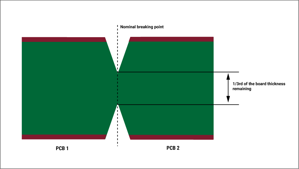
A V-score is a groove that is cut into a board material (the whole panel) between each copy of circuit boards. This mechanical process removes one-third of the PCB thickness from the top and another third from the bottom, leaving one-third for joining the boards in the middle. However, there’s a risk of the V-score cutting through the printed board rails within the array. We employ jump scoring on PCB panels to strategically introduce gaps in the V-score line, ensuring the array’s structural integrity.
The V-scores should appear as straight lines on the panel, which constrains the shape of the individual boards. Due to this limitation, tab routing has become more popular, as it allows cutting boards of any shape, while V-scoring is only feasible for square and rectangular PCBs.

Design for Manufacturing Handbook
11 Chapters - 96 Pages - 90 Minute ReadWhat's Inside:
- Annular rings: avoid drill breakouts
- Vias: optimize your design
- Trace width and space: follow the best practices
- Solder mask and silkscreen: get the must-knows
Download Now
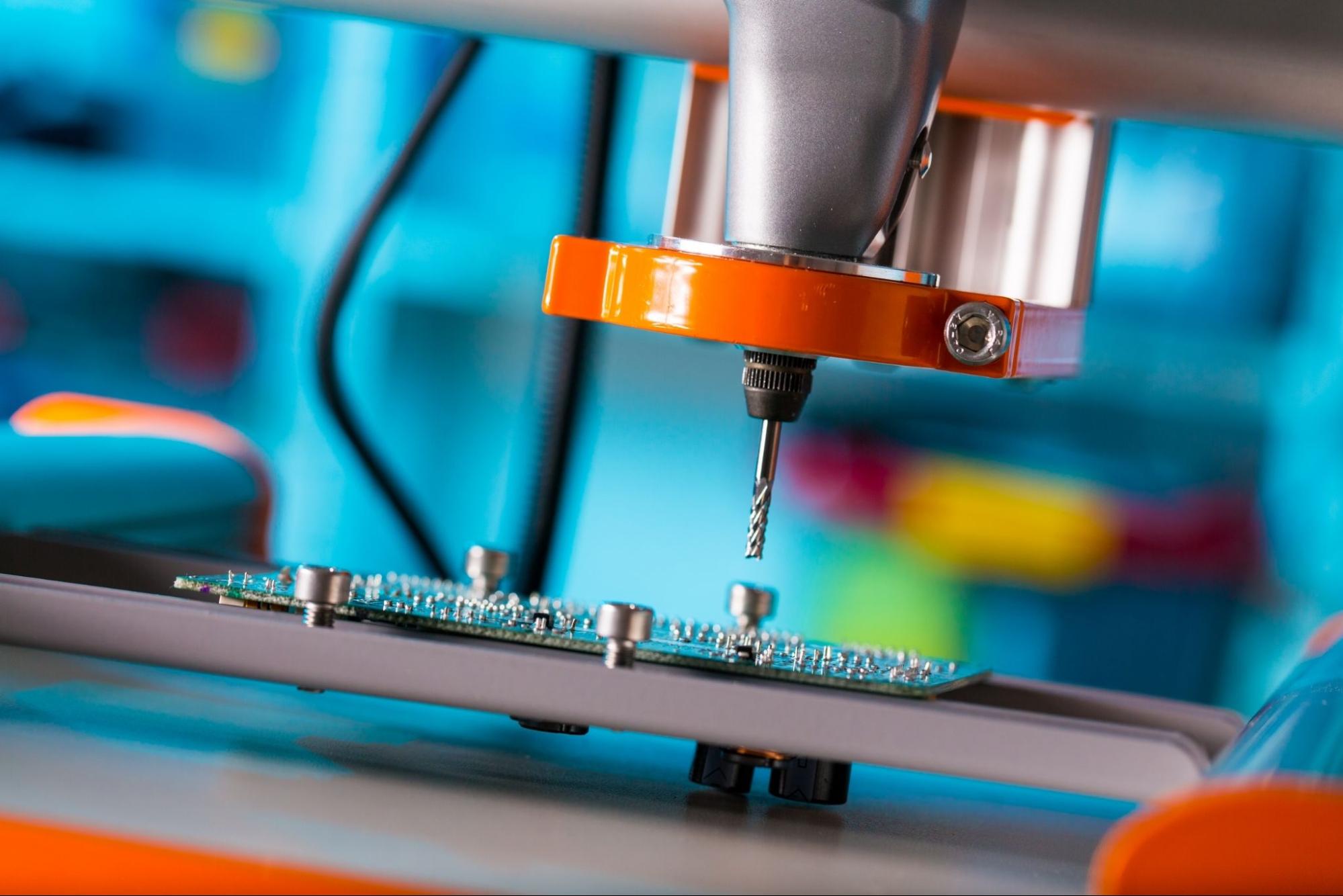
Milling
Milling is basically controlled depth routing where a specific amount of material needs to be removed. It is mostly used for pocket milling. From a simple recess on a board to a fully plated conductive structure connecting several layers, these structures can range from simple to complex. Additionally, it’s used for cutting cavities for heat sinks. The simple operations are done mechanically, but a laser is used when landing on underlying copper.
This PCB mechanical process is efficiently performed using a CNC machine/router. While the main drilling tool is the laser, we also have a Schmoll LM2-based drilling/routing system with vision, surface mapping, and depth control. The most important parameters are good registration and Z-axis depth control. Cutting and milling plated slots are accomplished with carbide end mills.
Back-drilling
Back-drilling (also known as controlled depth drilling) is a PCB mechanical process used to remove the stubs from plated through holes or vias. Stubs are undesirable portions of vias. They cause signal reflections and impedance discontinuities. Moreover, stubs will affect the signal integrity.
When circuit boards suffer from bit error rate (BER), deterministic jitter, signal attenuation, or other EMI problems, back drilling may be the best option. A long stub will result in severe signal distortion. Now, the question may arise: why is back drilling preferred over blind or buried vias to maintain high-speed signal quality? It is because back drilling has a lower cost than blind and buried vias. Furthermore, back drilling can also reduce manufacturing difficulty of boards significantly.
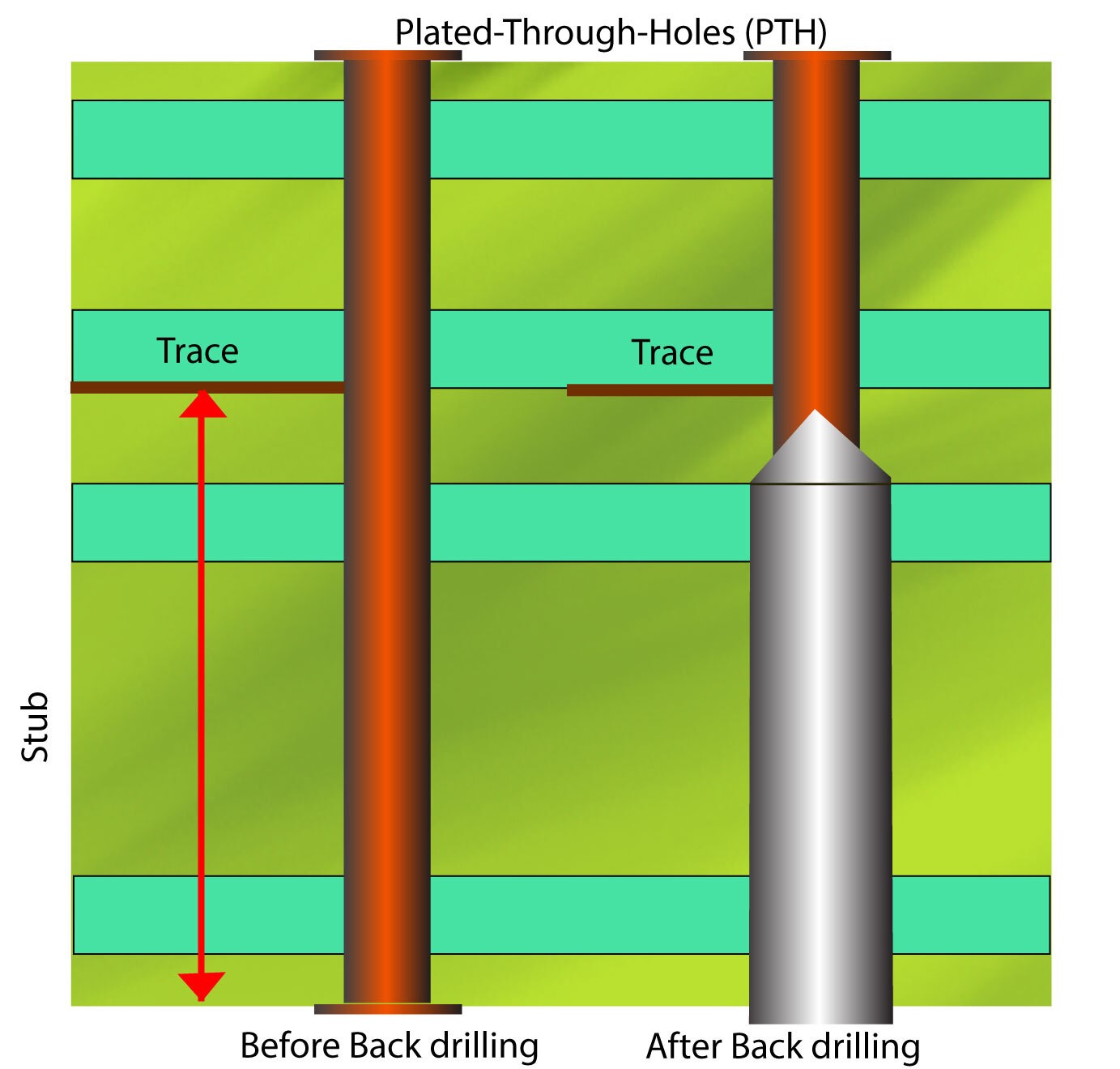
This process is performed using a computer-controlled drilling machine. Using a correct program, the operator will specify which drill to use based on the X-Y coordinate of the holes. Back drilling requires a larger drill bit than vias for the removal of conductive coatings or stubs. Drilling can be carried out using laser drilling or mechanical drilling. Laser drilling is more precise, and mechanical drilling is easier to use. Controlled depth drilling usually involves mechanical drilling.
The minimum tolerance for back drill is a stub of 10mil +/- 2mils. The trace to the tip is basically 10 mil.
The efficiency and accuracy of the PCB mechanical processes determine the success of fabrication. PCB manufacturers take maximum care and precision to carry out these activities to produce high-quality boards. Error-free equipment and neutral operating environments also contribute to the desired end result of these mechanical operations.
Try our free Better DFM tool and save time and money.
Our automated platform will catch any PCB design error ahead of time and prevent on-holds and re-spins. Get started by uploading your Gerber files here.


