


Contents

On-demand webinar
How Good is My Shield? An Introduction to Transfer Impedance and Shielding Effectiveness
by Karen Burnham
PCB trace termination is crucial for maintaining signal integrity in your designs. Unterminated traces can lead to issues like impedance discontinuities, signal reflections, crosstalk, and increased power consumption.
By strategically placing termination resistors at either the source or load, impedance mismatches can be balanced out. This approach ensures efficient signal transmission and reduces potential problems.
Highlights:
- Appropriately terminating traces ensures consistent impedance, minimizing signal distortion at the transmitter and the receiver end.
- Series termination involves placing a resistor in series close to the source to match the driver’s impedance with the line impedance.
- Parallel/shunt termination involves placing a termination resistor in parallel with the receiver at the load end, providing a low-impedance path for reflected signals.
- Calculating the reflection coefficient helps predict the severity of signal reflections.
In this article, you will learn the important trace termination techniques to maintain signal integrity in your designs.
You can also watch the full webinar here: PCB trace termination techniques to ensure signal integrity
4 reasons to terminate signal lines in your circuit board
1. Ensures uniform impedance
Each trace has a specific characteristic impedance depending on its shape and dielectric properties. If a trace is left unterminated, the transmitter or receiver impedance may not match the transmission line’s impedance.
You can achieve consistent impedance and minimize signal distortion by employing circuit board trace termination techniques.
2. Reduces signal reflections
The signal encounters an impedance discontinuity when a trace ends without a proper termination. This mismatch causes the signal to bounce back, traveling in the opposite direction. These reflections can distort the original signal, resulting in various issues such as:
- PCB ringing: The reflected and original signals bounce back and forth, creating an oscillating waveform.
- Overshoot: The reflected wave can produce a voltage spike that exceeds the signal’s maximum amplitude.
- Undershoot: The reflection may also cause a voltage drop below the intended level.
- Timing skew: As the reflected signal returns along the trace, it can interfere with subsequent signal transitions, causing delays and disrupting overall signal timing.


Sierra Circuits can deliver your circuit boards with a 5% impedance tolerance. Visit our controlled impedance capabilities to learn more.
3. Mitigates crosstalk and EMI
Unterminated traces act like small antennas, radiating electromagnetic waves. These waves can couple with nearby traces, inducing unwanted currents in them. Terminating the signal lines reduces the emission of EM radiation and crosstalk.
To learn how to minimize crosstalk in your layout, see handling crosstalk in high-speed PCB designs.
4. Optimizes power consumption
Signal reflections caused by unterminated traces dissipate more energy and increase power consumption. To avoid this, terminate the trace with a resistor that matches the characteristic impedance.
The termination resistor absorbs the signal energy, eliminating the additional power loss associated with reflections.
Download this eBook to learn how to design reliable transmission lines for your printed circuit board.

PCB Transmission Line eBook
5 Chapters - 20 Pages - 25 Minute ReadWhat's Inside:
- What is a PCB transmission line
- Signal speed and propagation delay
- Critical length, controlled impedance and rise/fall time
- Analyzing a PCB transmission line
Download Now
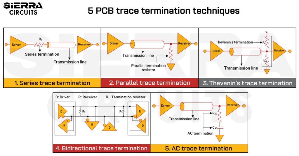
5 PCB trace termination techniques
1. Series trace termination
This method involves placing a resistor in series between the driver and transmission line. Ideally, you must position this resistor close to the source and match the driver’s impedance with the characteristic impedance of the trace.

Choosing the right series termination resistor
When selecting the resistor value, ensure that the sum of the driver impedance (Zsource) and the resistor impedance (Ztermination) equals the line impedance (Ztrace).
Mathematically, this can be expressed as Zsource + Ztermination = Ztrace
For instance, let’s consider a scenario where the Zsource is 23 Ω, and the Ztrace is 50 Ω.
To achieve impedance matching, Ztermination is calculated as follows:
Ztermination = Ztrace – Zsource = 50 Ω – 23 Ω = 27 Ω

The graph below shows the oscilloscope waveforms for different series termination resistors. Let’s assume the driver impedance is 23Ω and the line impedance is 50Ω. To match these impedances, 4 series termination resistors are incorporated with the values of 10Ω, 22Ω, 33Ω, and 47Ω.

Overshooting will occur if the sum of driver and termination impedances is less than the line impedance. This can be observed in the waveform for 10Ω and 22Ω resistors.
If the total impedance of the driver and termination resistor is higher than the line impedance, it results in undershooting in the waveform. Refer to the waveforms for 33Ω and 47Ω.
Always choose a termination resistor that balances driver and line impedances to minimize overshooting and undershooting. In this case, selecting a 33Ω resistor achieves this balance more effectively than others.
Differential series termination
In differential signaling, a series resistor is placed in series with each signal line of a differential pair close to the driver. This technique minimizes driver power dissipation while offering similar benefits to single-ended series termination.
A series resistor helps achieve a critically damped state in signal transmission and the fastest settling time without overshoot or oscillation. These resistors ensure the signal reaches the desired logic level smoothly.

In this process, you can employ an RLC model to calculate the transient oscillation frequency and damping. By knowing the load capacitance and inductance, you can precisely calculate the value of the series termination resistor needed to achieve critical damping: Z = 2 √L/C

Benefits of implementing series termination resistors
- The series termination resistor provides a good noise margin with low power consumption.
- Requires only a single resistor, simplifying your PCB layout.
- Helps achieve a critically damped state in signal transmission, minimizing overshoot and oscillation.
While series termination offers numerous benefits, however, it slightly delays signal propagation time. This propagation delay may not be significant in most cases, but it’s a factor for high-speed designs.

2. Parallel/shunt termination
Parallel termination minimizes signal reflections at the load end of a transmission line. It involves placing a termination resistor in parallel with the receiver. It also provides a low-impedance path for any reflected signals.

Typical values of shunt termination resistors are 50 or 75Ω. Placing them close to the receiver is crucial for optimal performance and minimizing signal degradation.
This method is commonly used in high-speed data interfaces such as DDR memory, PCIe, Ethernet, and USB applications.
For efficient routing strategies, see 11 best high-speed PCB routing practices.
Differential parallel termination
Here, a resistor is added in parallel to each differential signal line, as shown below.
This configuration addresses all differential reflections but may not eliminate common-mode reflections. However, this technique increases the drive current and may create trace stubs, resulting in signal integrity issues.

Benefits:
- No additional signal delay: Unlike series termination, parallel termination does not introduce any additional time delay or change in signal rise time.
- Suitable for daisy chain topologies: Parallel termination is well-suited for daisy chain configurations where multiple devices, such as DDR memory modules, are connected in series along a single transmission line.

Parallel termination typically incurs higher power consumption than series termination due to the continuous flow of shunt signals to the ground or power supply.
The Sierra Circuits design team effectively addressed signal reflection issues while working on a complex design involving four DDR3 memory chips connected to an FPGA memory controller.

The team implemented parallel termination with a 35.7 Ω shunt pull-up resistor at the end of the last DDR rather than placing four termination resistors at each DDR (as shown in the image above). This streamlined approach reduced trace stubs and improved signal integrity across 25 address lines.
This strategy resulted in efficient signal transmission, minimized data corruption, and ensured reliable performance across all DDR3 memory modules.
For more such tailored technical solutions, partner with us. Book a meeting with a design expert.
3. Thevenin’s trace termination
Thevenin’s termination utilizes Thevenin’s equivalent circuit to match the impedance of the transmission line.
The circuit typically consists of two resistors parallel to the signal trace. The values of the resistors are chosen such that the circuit’s impedance is equal to the trace’s impedance.

Benefits:
- Reduced signal attenuation: Thevenin’s termination minimizes signal attenuation along the transmission line, ensuring the signal reaches its destination with minimal loss.
- No timing delay: Unlike other termination methods, Thevenin’s termination does not introduce any timing delays in signal transmission.
- Level adaptation: It allows for level adaptation, enabling adjustment of signal levels between different circuit stages without significant signal degradation.
Drawbacks:
- Increased power consumption: Compared to alternative termination methods, Thevenin’s termination may consume more power due to the additional resistors involved in the circuit.
- Higher cost: Including extra resistors in the circuit adds to the overall cost of your circuit board.
- Space constraint: Thevenin’s termination circuitry occupies additional space on the board, which can be a constraint in compact designs.
4. AC PCB trace termination
AC termination introduces capacitors in series with parallel terminating resistors, offering advantages in various applications.
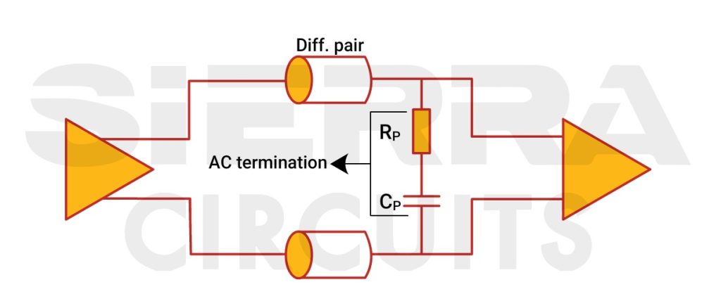
Differential AC termination
In differential AC termination, a resistor and a capacitor are combined in series at the end of each trace in the differential pair.
Therefore, this approach reduces the DC current loop, making it suitable for low-speed control lines.
Benefits:
- Wider frequency range: The capacitor-resistor combination offers effective termination over a wide frequency range. Therefore, it is suitable for high-speed digital signals and analog applications.
- Adaptability: AC termination allows the circuit to adapt to dynamic changes in signal voltage levels and is suitable for applications with varying data rates.
Drawbacks:
- Complexity and cost: While AC termination offers advantages, implementing it may result in a more complex circuit design, leading to additional costs for components and manufacturing.
- Power consumption: AC termination consumes more power than passive termination methods due to capacitors’ continuous charging and discharging.
- Component sensitivity: It is sensitive to component value and tolerance variations.
For more on high-speed and high-current PCB trace design, see the 10 best layout tips for high-speed and high-current PCB traces.
5. Bidirectional termination
Bidirectional trace termination extends the concept of parallel termination to facilitate multipoint communication on the same trace and enable multiple devices to transmit and receive data. Here, 2 termination resistors (RT) are placed at the extreme ends of the transmission line, parallel to the receiver, to minimize stub lengths and reduce signal reflections.
Bidirectional termination typically supports half-duplex transmission, where devices can transmit or receive data anytime.

Benefits of bidirectional trace termination
- Reduced power dissipation: Two termination resistors are used in bidirectional termination, effectively doubling the load on the driver. As a result, driver current and power dissipation increase, impacting the system’s overall power consumption.
- Improved noise margin: While bidirectional termination facilitates multipoint communication, it may reduce the noise margin as the driver output level decreases.
Despite several advantages, the bidirectional termination method is typically complicated compared to other techniques.
Download our e-book to learn how to design high-speed circuit boards with optimal signal integrity.

High-Speed PCB Design Guide
8 Chapters - 115 Pages - 150 Minute ReadWhat's Inside:
- Explanations of signal integrity issues
- Understanding transmission lines and controlled impedance
- Selection process of high-speed PCB materials
- High-speed layout guidelines
Download Now
Importance of the reflection coefficient in PCB trace designs
The reflection coefficient (Γ) measures the amount of signal reflection that occurs at the junction between a transmission line and a transmitter/receiver. It represents the ratio of the reflected signal’s amplitude to the incident signal’s amplitude. The coefficient is a complex number, where its magnitude indicates the proportion of the signal that reflects, and its phase indicates the polarity of the reflection.
Calculating the reflection coefficient helps you to:
- Predict the severity of signal reflections caused by impedance mismatches
- Design an appropriate termination strategy to minimize reflections
- Decide on the right resistor values
Here’s an example of a transmission line schematic:

Where
Zsource is the source impedance; Ztrace is the transmission line impedance; Zload is the receiver impedance
Here’s the formula to calculate it:
Γ = (Zload – Ztrace) / (Zload + Ztrace)
The reflection coefficient can take on different values between 0 and 1, each signifying a specific situation:
Condition 1: Γ = 0
This represents a perfect match between the characteristic impedance (Zo) of the trace and the impedance (ZL) of the connected component (transmitter/receiver). In this ideal scenario, there is no impedance mismatch. Hence, all the signal energy is transmitted, resulting in no reflections.
Condition 2: Γ = 1
This signifies a total reflection. The entire signal bounces back because the connected component encounters a very high impedance (open circuit) or a very low impedance (short circuit) compared to the trace impedance. This situation is highly undesirable and should be avoided through proper termination.
Condition 3: 0 < Γ < 1
This indicates a partial reflection. Only a portion of the signal reflects, while the remaining portion continues to the connected component. The severity of the reflection depends on the specific value of Γ.
The reflection coefficient is a complex number and includes a phase angle, providing additional information about the reflected signal:
0° or 180° phase angle: These values indicate a reflection that causes overshooting.
90° phase angle: This signifies a reflection that leads to undershooting.
Key takeaways:
- Transmission line trace termination ensures undistorted signal transmission and mitigates signal integrity issues.
- Trace termination techniques such as series, parallel, Thevenin’s, AC, and bidirectional termination minimize reflections by matching impedance and absorbing reflected signals.
- Series termination offers low power consumption and a simple design but introduces a slight signal delay.
- Parallel termination is suitable for daisy chain topologies but consumes more power.
- Thevenin’s termination reduces signal attenuation and allows level adaptation but increases cost and complexity.
- AC termination offers a broader frequency range and adaptability but requires more complex circuitry.
- Bidirectional termination facilitates multipoint communication but comes with increased complexity and a reduced noise margin.
PCB trace termination is crucial in high-speed designs to ensure signal integrity and reliable data transmission. When there is an impedance mismatch between the transmission line and the connected components, high-speed signals can suffer from issues such as reflections, overshoot, and undershoot.
Employing appropriate termination methods, as discussed in this article, can achieve optimal performance, reduce errors, and improve overall system stability. When implementing terminating resistors, you must carefully evaluate the trade-offs among signal integrity, power consumption, and noise margin.
Need assistance in routing your high-speed signals? Post your queries on our PCB forum, SierraConnect. Our design and manufacturing experts will resolve them.

About Poulomi Ghosh : Poulomi is a microwave engineer specializing in EMI, EMC, RF, and high-speed electronics. As a senior technical writer at Sierra Circuits, she creates advanced engineering articles and webinars for hardware engineers and PCB designers.


Great article, Poulomi!
Thanks, Lucy!