Solder mask refers to a thin coating of polymer that is applied on a PCB to shield the copper from oxidation and shorts. This layer also protects the board from dust or other contaminants that may cause shorts during operation.
What are the types of solder masks?
The different types of solder masks include:
Top and bottom side masks: This is used to detect openings in the green solder mask, post-application. It is applied using epoxy or film methods.
Epoxy liquid solder masks: They are made of a polymer that is applied with a method known as silkscreening. It’s a cost-effective option.
Liquid photoimageable (LPI) solder masks: They consist of a mix of different polymers and solvents that are stored as two different liquids until actual application.
Dry film photoimageable solder masks: This requires vacuum lamination and is used for high-density wiring boards. The process involves exposure of the dry film followed by development.

Design for Manufacturing Handbook
11 Chapters - 96 Pages - 90 Minute ReadWhat's Inside:
- Annular rings: avoid drill breakouts
- Vias: optimize your design
- Trace width and space: follow the best practices
- Solder mask and silkscreen: get the must-knows
Download Now
Solder mask clearance
Solder mask clearance decides how close the solder mask can be to the board surface features. The purpose of this tolerance is to implement sufficient spacing known as solder dams between board surface features that receive solder. In PCB design, solder mask defined (SMD) and non-solder mask defined (NSMD) pads are crucial as they determine how solder mask clearances are managed, impacting soldering precision and potential issues like short circuits.
Conventionally, solder mask clearance is required to be half the conductor spacing width. For the fine conductive patterns, the solder dam should be 100µm (4 mils) or more.
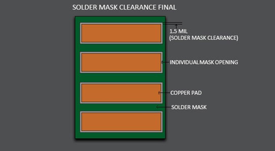
The solder mask process calls for fitting tolerances that have the mask clearance greater than the solder pads. This is needed to ensure optimal soldering and keep the full pad free of solder resist.
Solder mask opening
The outer layer regions of the board without the mask are known as the solder mask opening. This opening is used to expose the PCB to solder/tin. It needs to be precise, or it might unnecessarily expose the copper on the board, causing corrosion and damage.
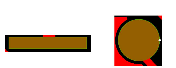
Traditionally, manufacturers opt for 1:1 solder mask openings with copper pads. It can be changed according to the relevant fabrication process. The opening has to be tailored to the requirements, or it might expose the ground plane next to the pad. This can cause shorts and needs to be prevented.
What is paste mask expansion?
Electronic design automation software (PCB design tools) conventionally allows designers to specify the spacing between surface features and solder mask on the board. This parameter is generally referred to as solder mask expansion and can be a positive, negative, or typically zero value.
What is solder mask relief or solder mask web?
The area on the board surface that does not need or have a solder mask is known as solder mask relief. Such areas are typically present around test points, through-hole pads, vias, and SMT pads to act as a margin of error during fabrication. For example, many EDA software look for a minimal opening of 8µm (0.315 mils) larger than the pad, by default. On each side, this comes up to 4µm (0.1575 mils) relief.
Common solder mask errors
Solder bridging
It refers to the formation of an unintended connection between two solder junctions. This problem could be caused due to various design errors, such as a lack of space between the solder mask layer and the surface mount pad, or misalignment of components. For optimum solderability, refer to the IPC standards on pad dimensions.
Solder bridging can still happen despite all of the precautions. If it occurs, use a thin tip solder iron, wet it with solder paste, and heat the solder bridge to repair this. Drag the heated solder off the pads gently. Then, using a multimeter, check to see if the pads are still shorted.
Tombstoning
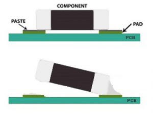
A tombstone is a chip component that has partially or completely been pulled off the pad into a vertical position, having only one end soldered. This occurs due to force imbalances during the reflow soldering process. Uneven heating, unequal heat sinks, and excess movement during and after the reflow operation are a few reasons for tombstoning. Below are a few possible solutions to avoid this.
- The component body must cover at least 50% of both pads.
- Maintain a high preheat temperature such that the reflow temperature disparity between the two ends is minimal.
- Minimize the movement during the SMT assembly to the least possible during reflow.
Cold solder joint (Excess solder)
This occurs when the solder does not completely melt. Cold solder joint occurs due to:
- Lengthy leads
- Presence of excess solder on the board
- If the solder between the component lead and the pad did not wet properly.
Solder balling
Solder balls are formed by flux gassing on the wave’s surface or by solder bouncing back from the wave. These are caused by excessive soldering temperatures, splash-back of solder driven by gas release during the soldering process. To avoid solder balling, the preheat temperature should be set accurately. If there are discrepancies in preheat temperature, the quantity of flux applied increases, which in turn affects the evaporation of the solvent from the flux.
For more details, read our post what is solder mask?


