What is wave soldering?
Wave soldering is an extremely effective method for soldering printed circuit assemblies (PCAs). In this process, components are mounted on PCBs by inserting their leads into holes (through holes) extending from one side of the board to the other.
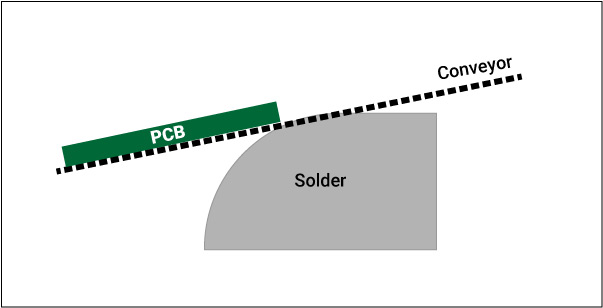
Once all the components have been mounted, a conveyor moves the assembly over a horizontal mound of solder flowing across beneath the circuit board. The solder connects the component leads to the pads that surround the holes.
How it began
Wave soldering originated in the late 1950s as an elegant solution to a messy problem brought on by a technological breakthrough in electronics. Up until the mid-1950s, most electronic components were vacuum tubes, devices that look like light bulbs but have electrodes instead of filaments. The tubes were inserted into sockets mounted on a chassis (a supporting plate). Wires soldered to tabs on the sockets provided the electrical circuitry. All soldering was done manually.
With the advent of solid-state components and PCBs, the leads of these new components dropped right into holes in the board. The holes were surrounded by pads on the bottom of the circuit board and tracks replaced the wiring that had been required to connect vacuum tube sockets. The electrical circuit was completed by soldering the component leads to the pads.
These early PCBs were known as single-sided boards because all the circuitry was on just one side and the component bodies resting on the other side. They became more complex over time. The next generation gave rise to double-sided boards that added metal plating to the walls of the holes (plated through-holes) allowing connection to circuitry on the component side when filled with solder. Multilayer PCBs with internal traces joined by tiny plated holes (vias) came next. Pure through-hole assemblies increasingly gave way to hybrid assemblies that combined through-hole and surface mount components. And, most recently, rigid PCBs were joined by flexible circuitry. But mass soldering all began with those first crude single-sided assemblies.

Soldering Flux eBook
13 Chapters - 24 Pages - 40 Minute ReadWhat's Inside:
- Why flux is needed
- The ingredients of flux and what they do
- Soldering flux categories
- How to read a flux manufacturer’s technical data
- The best flux for various applications
Download Now
How does wave soldering work?
Wave soldering is an efficient soldering method for PCBs containing many through-hole components and large connectors with very high pin counts. In this process, the boards are passed over a wave of molten solder. This includes solder fluxing, preheating, solder waves, and cooling.
Wave soldering design considerations
To achieve a proper solder joint, it is necessary to focus on a few design considerations.
Solder pad mask opening
The solder pad mask opening of a board can be of two types: solder mask defined (SMD) and non-solder mask defined (NSMD). In wave soldering, the SMD pad is preferred because the mask serves as an added spacer between the component and the board pad. This allows more room for flux to flow and easy filling of solder in the space between component terminations and board. NSMD is used for through-hole components while SMD is used for ICs.
Surface finish
There are two types of surface finishes compatible with wave soldering: hot air solder leveling (HASL) and organic solderability preservatives (OSP). In HASL, easy solder filling is observed. OSP is inferior in wetting compared to HASL but produces consistent thin coatings. The proper choice of solder flux can help OSP to achieve appropriate wetting.
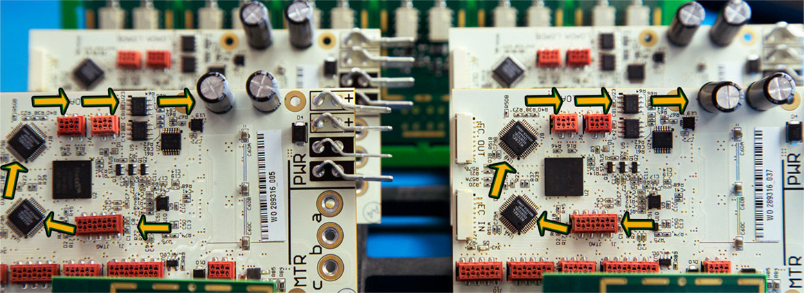
Tips for component placement and orientation for wave soldering
- Surface mount components should not be placed too close to through-hole components. It may block the through-hole pins from the full force of the solder wave. As a result, through-hole pins will have a poor solder connection.
- Smaller components should not be placed behind larger ones. It could result in larger components shadowing the smaller ones, and this leads to improper solder joints.
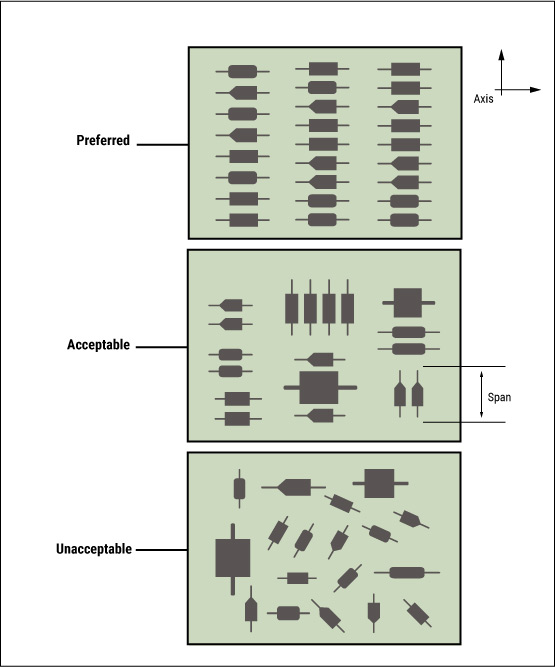
- Multi-pin SMT parts such as ICs should be placed in line with the direction of the wave to avoid shadowing the trailing pins.
- The land pad dimensions should be larger than the nominal footprint dimension. It is best to follow the IPC specifications while designing PCB footprints.
Component clearances
Components should have adequate spacing in between them to have a properly soldered connection. It is crucial to place the parts where they will be accessible for any kind of rework required in later stages.
Pad shapes
Pad shape is a concern for fine-pitch SMTs while performing wave soldering. When the solder wave reaches the end of a part, the sudden change can cause excess solder to accumulate on the last few pads, resulting in solder bridges. To protect against this issue, thieving pads are added at the ends of these components to collect any excess solder as the wave passes. These pads should extend from the last functional pads that the solder wave will touch; it is common to use thieving pads for surface mount packages.
Solder flux
Appropriate flux selection is very important in this process. Flux removes oxides and prevents the formation of new oxides until the solder is applied. Solder flux used in PCB assembly contains acids (activators), materials (solids) to prevent oxygen from reaching the deoxidized metal, and solvents to make the application of the flux easier. Solder flux can be used with low solid content or high solid content for facilitating solder wetting. The flux can be applied either with spraying or foaming.
How to take a wave soldering profile
In this process, preheat temperatures and preheating time should be set according to the flux specifications. The flux activation system may cause shorts due to high preheat temperatures and long preheat times. Conversely, too low preheat temperature may result in skips or unwanted residues left on the circuit board.
For more details read, making sense of wave soldering by Jim Smith.


