PCB fabrication notes serve as the primary communication channel between the designers and fab houses.
They are generally added to fabrication drawings, which comprise the board shape with dimensions, location of the drilled holes (drill chart), details of cut-outs, layer stack-up, and title block.
Here, you’ll learn how to effectively create fab notes to ensure desired circuit board manufacturing. You will also see an example of comprehensive fab notes that will help you clearly convey your specific fabrication requirements.
What are fab notes in PCB design and manufacturing?
PCB fabrication notes include:
- Specific manufacturing instructions
- Assembly notes
- Impedance requirements
- Solder mask and silkscreen specifications
- Circuit board manufacturing tolerances

As a PCB designer, it is crucial to clearly communicate your requirements to your fabricator to ensure the desired circuit board is built accurately and efficiently.
Fab notes include board data files such as IPC-2581 (unified design data), Gerber, and ODB++.
It also comprises drill files in text or PDF form.
To learn more about design for manufacturing, download our e-book.

Design for Manufacturing Handbook
11 Chapters - 96 Pages - 90 Minute ReadWhat's Inside:
- Annular rings: avoid drill breakouts
- Vias: optimize your design
- Trace width and space: follow the best practices
- Solder mask and silkscreen: get the must-knows
Download Now
Details to include in your circuit board fabrication notes
Here’s an infographic on what to specify in your fab notes:
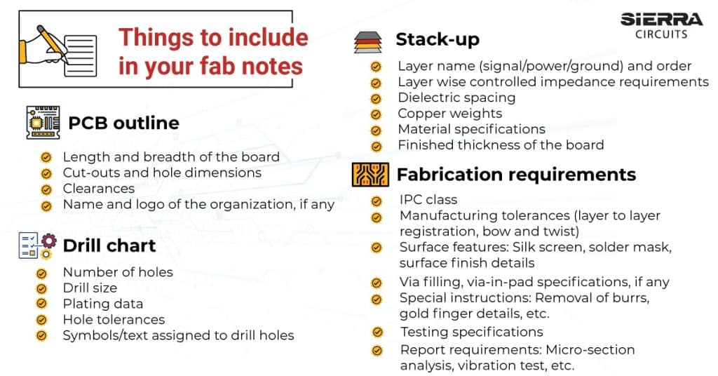
Fab notes should contain the following details:
- Drill sizes and tolerances
- Location of slots, notches, and cutouts
- Dimensions of the board in X-Y coordinates and the board outline
- Hole-to-edge dimensions for holes near the board edge
- The date of the drawing, version history and author
- Plating tolerances
- Solder mask and silkscreen specfication
- PCB surface finish requirements
- Presence of blind/buried vias
- Via-in-pad requirements
- Layer wise controlled impedance requirement (impedance table)
Here’s an example of impedance table:
| Layers | Impedance value | Trace width (mils) | Spacing (mils) |
|---|---|---|---|
| 1 and 10 | 50 ohms SE | 7.6 | - |
| 3 and 8 | 50 ohms SE | 4.6 | - |
| 1 and 10 | 100 ohms diff pair | 4.0 | 4.40 |
| 3 and 8 | 100 ohms diff pair | 4.0 | 8.0 |
| 5 and 6 | 100 ohms diff pair | 4.0 | 5.6 |
| 1 and 10 | 90 ohms diff pair | 5.0 | 4.0 |
| 3 and 8 | 90 ohms diff pair | 4.0 | 4.6 |
| 5 and 6 | 90 ohms diff pair | 4.2 | 4.0 |
| 5 and 6 | 50 ohms SE | 6,8 | - |
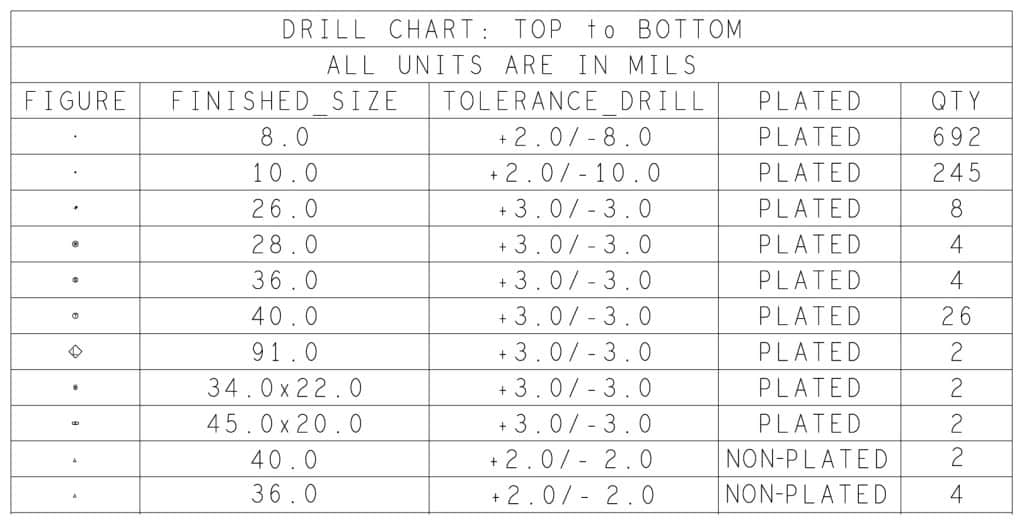
Here’s a typical drill chart that should be added to your fab notes.
The example fab note below will help you simplify your workflow, minimize errors, and accelerate your design process.
| Fabrication parameters | Requirements |
|---|---|
| IPC standard for medical PCB fabrication | IPC-6012EM, FDA |
| IPC standard for mil-grade PCBs | IPC-6012ES |
| IPC standard for automotive PCBs | IPC-6012EA, SAE, ANSI |
| PCB class | Class 1/Class 2/Class 3/Class 3A |
| Board material | FR4 |
| No. of Layers | 4 |
| PCB thickness | 62± 10% mil |
| Copper thickness on external layers | 1 Oz. finish copper |
| Copper thickness on internal layers | 1/2 Oz. finish copper |
| Solder mask color | Green |
| Surface finish | ENIG |
| Silkscreen | White |
| Blind & buried vias | Yes/No |
| Via-in-pad | Yes |
| Via filling | Conductive / Non-conductive |
| Impedance trace | Yes (See Impedance note) |
| Coverlay color | |
| Stiffener requirement (flex only) | Yes/No |
| Cut-out in design | Yes/No |
| Minimum plating thickness | 8 mil |
| PTH diameter tolerance | 3 mil |
| Board separation | Singulated/Panelized |
| Additional requirements | |
| Remove all burrs and sharp edges | |
| Teardrop internal and external pads on all signal nets, regardless of the annular ring size | |
Here are 10 exceptional specifications:
- The allowable warp or twist must not surpass 1%, according to the IPC-TM-650 2.4.22 standards.
- The hole position must not deviate more than 0.003 inches from the drill data location.
- Acceptable board outline tolerance is ±0.005”.
- The finished line width should not vary from the 1-to-1 master pattern image by more than ±0.025 mm or 20%, whichever is smaller.
- The bow and twist of the assembly sub-panel or singulated parts must not exceed 0.7% of the longest side.
- Test in accordance with the latest revision of IPC-TM-650 2.4.22.
- Adhere to RoHS-compliant processes and ensure Pb-free manufacturing.
- The layer-to-layer registration must be within a ±2 mil tolerance.
- The front-to-back registration should be within a tolerance of 5 mil.
- Cover all bottom vias with solder mask.
From standard specifications to rare requirements, our attention to detail ensures every aspect of your design is executed with precision.
To learn more about our expertise in circuit board fabrication, see our PCB manufacturing services.
9 guidelines to create effective fab notes
- Keep fabrication notes clear and concise. Avoid unnecessary vocabulary to prevent confusion.
- Do not include repetitive notes or values that may contradict each other.
- Make sure the values specified in the notes align with your manufacturer’s capabilities.
- Arrange the notes in the order corresponding to the sequence of fabrication processes. This facilitates a systematic checklist for the fabricator.
- The notes should be comprehensive so that the cost and turnaround time are minimal.
- Use clear and precise language to ensure the information is easy to understand for the PCB manufacturer.
- Ensure the notes specifically address details related to the fabrication process rather than focusing solely on the PCB’s overall functionality.
- Clearly indicate any deviations from the standard processes or capabilities provided by the manufacturer.
- Add revision history to highlight any updates made to the notes after the initial submission.
Fab notes serve as a communication channel between the PCB designer and the manufacturer, relaying important information about production processes and board features.
By clearly outlining your board specifications, fabrication requirements, and any special instructions, you can establish effective communication with the manufacturer.
This reduces the likelihood of errors, delays, and misunderstandings, ultimately leading to a seamless fabrication process and high-quality PCBs that align with your design expectations.


