
Speak to an Account Manager
 +1 (800) 763-7503
Microelectronics PCB Manufacturing and Assembly
Sierra Circuits manufactures micro circuit boards with 2-mil trace and space combined with microvias and ultra-thin substrates.

Why and where do you need microelectronic PCBs?
- Supports HDI architectures and fine-line routing.
- Handles high-speed signals with minimal loss.
- Facilitates advanced packaging and semiconductor integration.
- Enhances electrical performance while reducing overall system size and weight.
Ideal for:
- Consumer electronics – smartphones, fitness trackers, and portable devices.
- Telecommunications – 5G modules, RF, and IoT systems.
- Medical devices – implantables, diagnostic equipment, and wearable health monitors.
- Industrial electronics – sensors, control modules, and automation systems.

Why partner with Sierra Circuits for microelectronic PCB manufacturing?
- We manufacture advanced microelectronic circuit boards with ultra-fine features down to 2/2 mil, supporting HDI architectures, stacked/staggered microvias, and via-in-pad structures.
- We process advanced materials, including low-loss laminates, PTFE, and polyimides for RF and high-reliability applications.
- We use automated scaling systems, high-resolution LDI, and laser drilling to achieve precise layer registration and conductor geometries, ensuring consistent electrical performance across critical circuits.
- Through DFM reviews, we identify potential manufacturing issues and optimize trace widths, spacing, stack-ups, and via structures for a smooth transition from design to production.
- Our dedicated customer portal let’s to check your order status, track progress, access documentation, and stay informed at every stage.
Our expertise
- Blind vias, buried vias, and microvias
- Up to 5 lamination cycles
- 2 mil fine lines and 4 mil hole sizes
- Via-in-pad technology
- COIN services
- DFM and DFA analysis
| Stack-Up | Stack-Up | |||
|---|---|---|---|---|
| Minimum Layer Count | 1 | 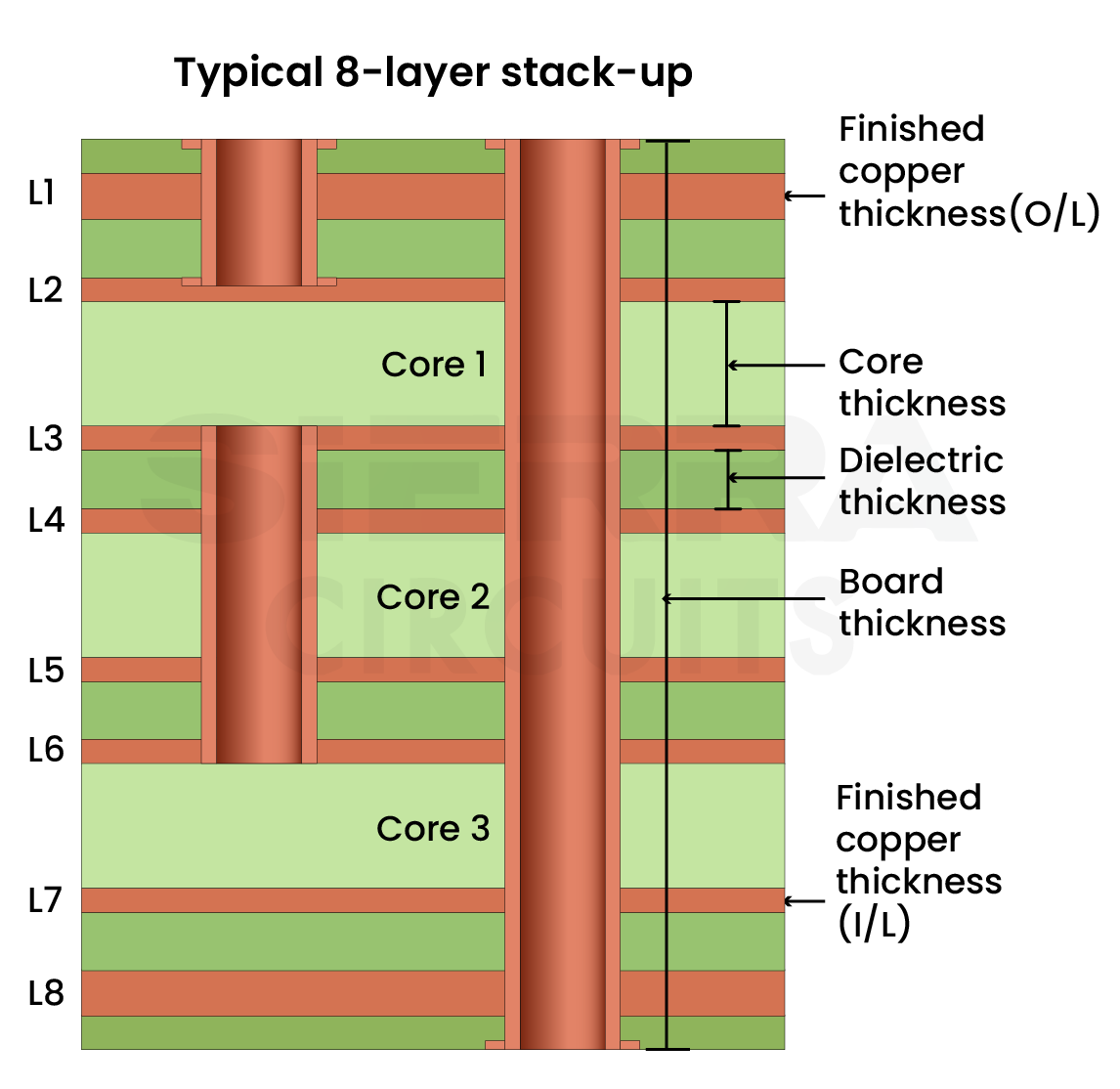 
| ||
| Maximum Layer Count | 36 | |||
| Minimum Board Thickness | 5 mil (0.0050 in/0.127 mm) | |||
| Maximum Boards Thickness | 300 mil (0.3000 in/7.620 mm) | |||
| Minimum Core Thickness | 2 mil (0.0020 in/0.051 mm) | |||
| Minimum Dielectric Thickness | 2 mil (0.0020 in/0.051 mm) | |||
| Minimum Starting Copper Foil Weight | 3 microns | |||
| Maximum Finished Copper Thickness (outer layer) | 1 oz | |||
| Maximum Finished Copper Thickness (inner layer) | 0.5 oz | |||
| Thickness Tolerance (based on board thickness) | ±10% | |||
| Hybrid Constructions | Yes | |||
| No Flow Prepreg | Yes | |||
| Bow and Twist Tolerance | Per IPC spec | |||
| Sequential Lamination | 5 lamination cycles | |||
| Drill and Pad | Drill and Pad | |||
|---|---|---|---|---|
| Minimum Finished Hole Size | 4 mil (0.0040 in/0.102 mm) | 
  | ||
| SmallestMechanical Drill Diameter | 5.9 mil (0.0059 in/0.150 mm) | |||
| Minimum Annular Ring-Mechanically Drilled | 2 mil (0.0020 in/0.051 mm) | |||
| Smallest Laser Drill Diameter | 4 mil (0.0040 in/0.102 mm) | |||
| Minimum Annular Ring-Laser Drilled | 2 mil (0.0020 in/0.051 mm) | |||
| Laser Hole Location Tolerance | 0.5 mil (0.0005 in/0.013 mm) | |||
| Blind Via Finished Hole Size | 4 mil (0.0040 in/0.102 mm) | |||
| Buried Via Finished Hole Size | 4 mil (0.0040 in/0.102 mm) | |||
| Stacked Vias | Yes | |||
| Conductive Filled Vias | Yes–Cu plate shut | |||
| Non Conductive Filled Vias | Yes | |||
| Maximum Through Hole Aspect Ratio (depends on the board thickness and finished hole size) | ≤20:1 | |||
| Maximum Laser Via Aspect Ratio | 0.75:1 | |||
| Minimum Pad Size for Test | 5 mil (0.0050 in/0.127 mm) | |||
| Process Pad Diameter | 4 mil (0.0040 in/0.102 mm) | |||
| Minimum Wire Bond Pad Size | 4 mil (0.0040 in/0.102 mm) | |||
| Backdrill to Copper Clearance | 0 mil (0.010 in/0.254 mm) | |||
| Backdrill to Backdrill Clearance | 6 mil (0.0060 in/0.152 mm) | |||
| Minimum Backdrill Oversize Diameter | 8 mil (0.0080 in/0.203 mm) to 10 mil (0.010 in/0.254 mm) | |||
| Minimum Controlled Depth Drilling | More than 1 mil (0.001 in/0.0254 mm) | |||
| Controlled Depth Drilling Tolerance | ±2 mil (0.002 in/0.0508 mm) | |||
| Minimum Pad to Minimum Mechanical Drill | Minimum Pad to Minimum Mechanical Drill | |||
|---|---|---|---|---|
| Mechanical Drill Size | Minimum Pad Size (2 × Annular ring + Drill size) |  | ||
| 6 mil (0.006 in/0.152 mm) | 10 mil (0.010 in/0.254 mm) | |||
| 7 mil (0.007 in/0.178 mm) | 11 mil (0.011 in/0.279 mm) | |||
| 8 mil (0.008 in/0.203 mm) | 12 mil (0.012 in/0.305 mm) | |||
| 9 mil (0.009 in/0.229 mm) | 13 mil (0.013 in/0.330 mm) | |||
| 10 mil (0.010 in/0.254 mm) | 14 mil (0.014 in/0.356 mm) | |||
| 11 mil (0.011 in/0.279 mm) | 15 mil (0.015 in/0.381 mm) | |||
| 12 mil (0.012 in/0.305 mm) | 16 mil (0.016 in/0.406 mm) | |||
| Minimum Pad to Minimum Class 3 Laser Drill | Minimum Pad to Minimum Class 3 Laser Drill | |||
|---|---|---|---|---|
| Laser Drill Size | Minimum Pad Size |  | ||
| 3 mil (0.003 in/0.0762 mm) | 7 mil (0.007 in/0.1778 mm) | |||
| 4 mil (0.004 in/0.1016 mm) | 8 mil (0.008 in/0.2032 mm) | |||
| 5 mil (0.005 in/0.1270 mm) | 9 mil (0.009 in/0.2286 mm) | |||
| 6 mil (0.006 in/0.1524 mm) | 10 mil (0.010 in/0.2540 mm) | |||
| 7 mil (0.007 in/0.1778 mm) | 11 mil (0.011 in/0.2794 mm) | |||
| 8 mil (0.008 in/0.2032 mm) | 12 mil (0.012 in/0.3048 mm) | |||
| Minimum Pad to Minimum Class 3 Laser Drill | Minimum Pad to Minimum Class 3 Laser Drill | |||
|---|---|---|---|---|
| Laser Drill Size | Minimum Pad Size | | ||
| 3 mil (0.003 in/0.0762 mm) | 9 mil (0.009 in/0.2286 mm) | |||
| 4 mil (0.004 in/0.1016 mm) | 10 mil (0.010 in/0.2540 mm) | |||
| 5 mil (0.005 in/0.1270 mm) | 11 mil (0.011 in/0.2794 mm) | |||
| 6 mil (0.006 in/0.1524 mm) | 12 mil (0.012 in/0.3048 mm) | |||
| 7 mil (0.007 in/0.1778 mm) | 13 mil (0.013 in/0.3302 mm) | |||
| 8 mil (0.008 in/0.2032 mm) | 14 mil (0.014 in/0.3556 mm) | |||
| Trace and Spacing Clearances | Trace and Spacing Clearances | |||
|---|---|---|---|---|
| Minimum Trace Width | 2 mil (0.0020 in/0.051 mm) |  | ||
| Minimum Trace Space | 2 mil (0.0020 in/0.051 mm) | |||
| Controlled Impedance Tolerance | ±10% | |||
| Minimum Etching Guidelines | 4.25 mil (0.00425 in/0.108 mm) spacing and 4 mil (0.0040 in/0.102 mm) trace width for 1 oz | |||
| Solder Mask and Surface Finish | Solder Mask and Surface Finish | |||
|---|---|---|---|---|
| Solder Mask Colors Available | Green and Red |  | ||
| Solder Mask Registration | 1 mil (0.0010 in/0.025 mm) | |||
| Solder Mask Feature Tolerance | 1 mil (0.0010 in/0.025 mm) | |||
| Solder Mask Minimum Dam Size (based on green solder mask color) | 3 mil (0.0030 in/0.076 mm)- 4 mil (0.0040 in/0.102 mm) for Green and Red | |||
| Solder Mask Finish | Semi–Glossy, Glossy and Matte | |||
| Legend Colors Available | All Colors | |||
| Surface Finishes Available | OSP, ENIG, Electrolytic Soft Gold, Electrolytic Hard Gold, Selective Gold | |||
| Mechanical Parameters | Mechanical Parameters | |||
|---|---|---|---|---|
| Minimum Panel Size | 12”x18” |     | ||
| Maximum Panel Size | 18″x24″ | |||
| Laser Routed Part Size Tolerance (Available for panels <0.032” thick) | 3 mil (0.0030 in/0.076 mm) | |||
| Minimum Diameter Route Bit | 21 mil (0.021 in/0.533 mm) | |||
| Routed Part Size Tolerance | 3 mil (0.0030 in/0.076 mm) | |||
| Routed Array | Yes | |||
| V Score, Edge to Copper | 7 mil (0.0070 in/0.178 mm) | |||
| V Score Angles | 35°, 45°, 60° | |||
| Countersink | Yes | |||
| Counterbore | Yes | |||
| Bevel | Yes | |||
| Milling | 1 mil (0.0010 in/0.025 mm) | |||
| Edge Castellation | Yes | |||
| Edge Plating | Yes | |||
| Heatsinks | No | |||
| Recommended Laminate Materials | Recommended Laminate Materials | ||||
|---|---|---|---|---|---|
| Isola 370HR | Panasonic Megtron | EMC 890 | |||
| Isola FR406 | EMC 370Z | Tachyon 100G | |||
| Isola FR408 HR | EMC 528 | ||||
| PCB Testing and Reports | PCB Testing and Reports | |||
|---|---|---|---|---|
| Electrical Testing | 10 Volt, 40 Volt (burn-in boards), 250 Volt, 500 Volt and Hi Pot |  | ||
| Microsection | Yes | |||
| Solderability | Yes | |||
| X-Ray Fluorescence | Yes | |||
| Ionic Contamination | Yes | |||
| Time Domain Reflectometry Test (TDR) | Yes | |||
| Wire Bond Testing | Yes | |||
| First Article Inspection (FAI) | Yes | |||
| Certificate of Compliance | Yes | |||
| PCB Certification | PCB Certification | |||
|---|---|---|---|---|
| MIL-PRF-55110 | Yes |  | ||
| MIL-PRF-31032/1 | Yes | |||
| MIL-PRF-31032/2 | Yes | |||
| IPC 6012, Class 1, 2 and 3 | Yes | |||
| ISO 9001:2015 | Yes | |||
| ISO 13485:2016 | Yes | |||
| UL (94VO) | Yes | |||
| AS9100 | Yes | |||
How to Place an Order for Microelectronic PCBs

Trusted by innovators
Engineers at the worlds most innovative companies choose Sierra Circuits for the highest quality microelectronic PCB manufacturing and assembly, right here in the USA.


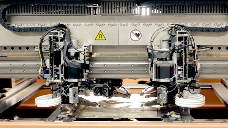
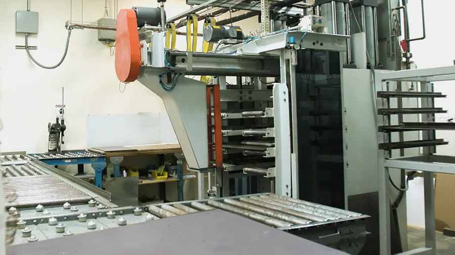

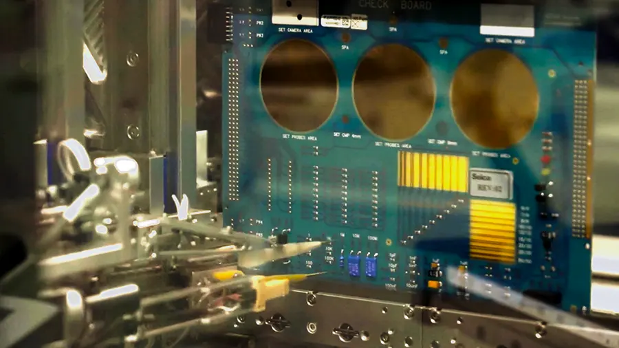



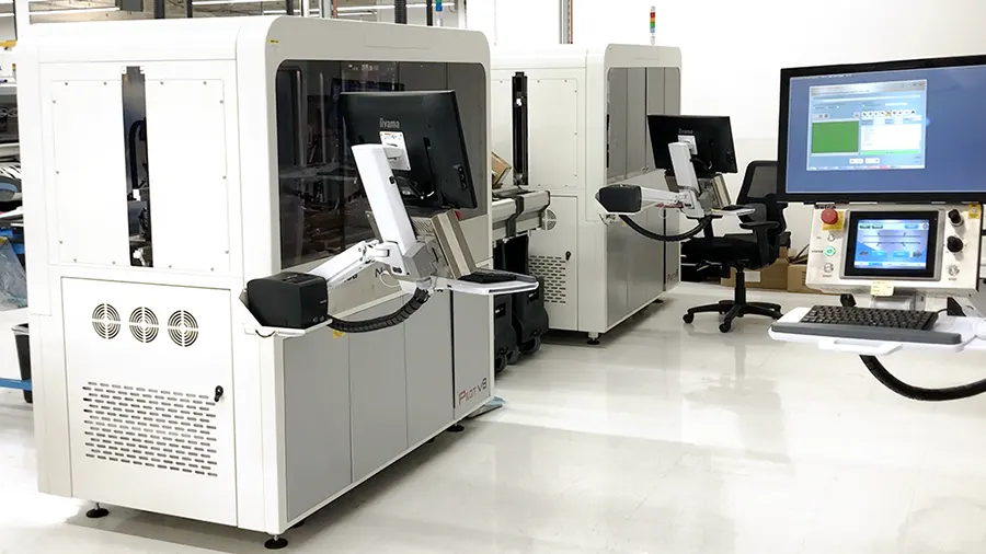
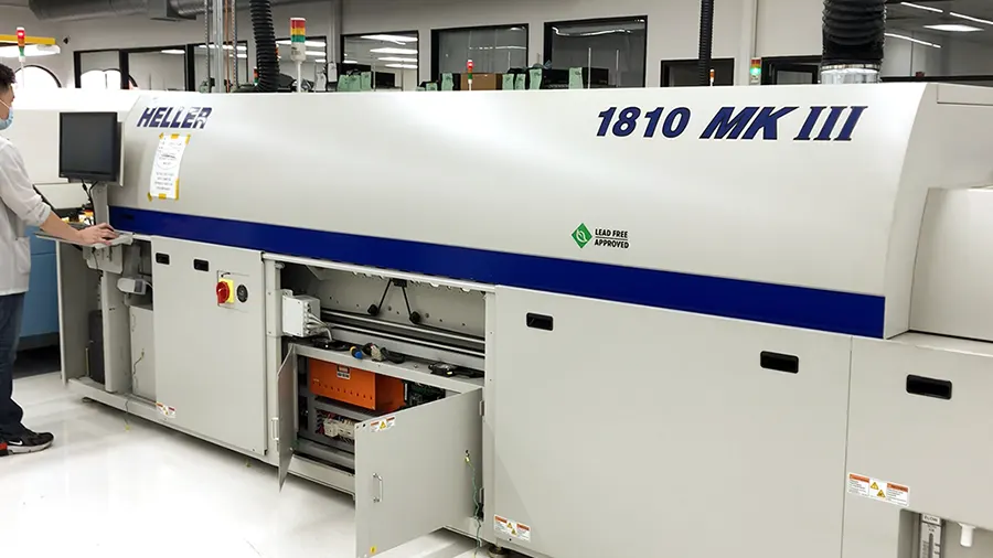
Manufacturing Equipment at Sierra Circuits
Our 70,000 sqft state-of-the-art campus in the heart of Silicon Valley contains the most advanced equipment required for the manufacture and assembly of your PCBs. Whether you’re looking for standard quick turn PCBs or boards with the tightest tolerances, made from exotic metals, there’s a reason Sierra Circuits leads the industry in quality and performance.



Fabrication, Procurement, & Assembly. PCBs fully assembled in as fast as 5 days.
- Bundled together in an entirely-online process
- Reviewed and tested by Engineers
- DFA & DFM Checks on every order
- Shipped from Silicon Valley in as fast as 5 days

Fabrication. Procurement & Assembly optional. Flexible and transparent for advanced creators.
- Rigid PCBs, built to IPC-6012 Class 2 Specs
- 2 mil (0.002″) trace / space
- DFM Checks on every order
- 24-hour turn-times available

Complex technology, with a dedicated CAM Engineer. Stack-up assistance included.
- Complex PCB requirements
- Mil-Spec & Class 3 with HDI Features
- Blind & Buried Vias
- Flex & Rigid-Flex boards