Case 1: If the PCB designer provides a wide annular ring area, chances are that the via will be drilled approximately in the middle of the pad. Even though it will not be dead-center, this will still retain a good electrical connectivity.
Case 2: If the designer doesn’t provide enough ring area, then the hole could almost end up touching the boundaries of the pad. This leads to an annular ring width that equals 0. Here, the drilled hole forms a tangent with the outer rim of the ring. This is called tangency. This will lead to connection problems between the via and the copper traces. This violates class 3 requirements.
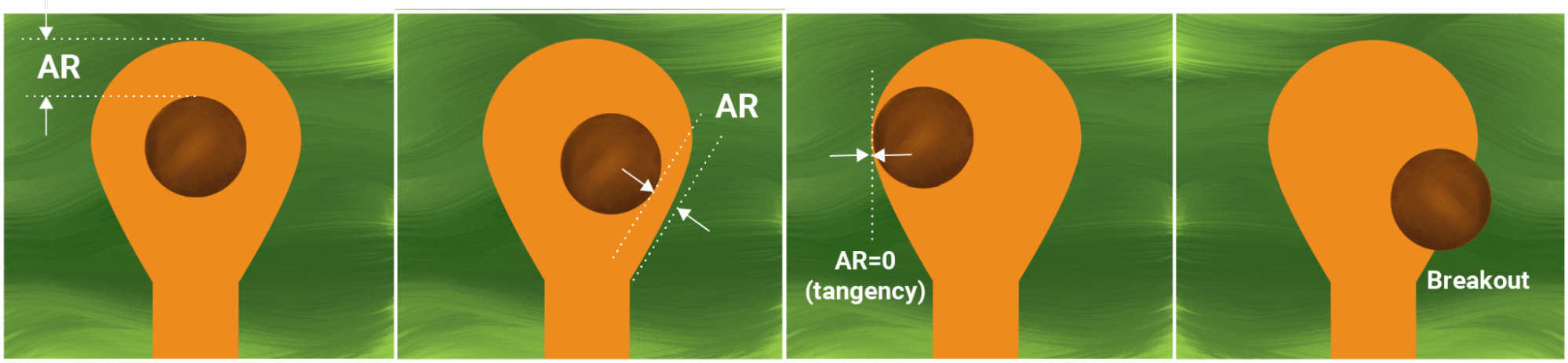
Case 3: The drill bit might deviate outside the pad during the drilling process. This is what we call an annular breakout. Annular breakouts can lead to connection problems between the via and the layers. It will also cause difficulties with component placement, solderability, and so on. If the drill breaks out of the pad, you could have a direct short. This is why you need an 8-mil drill-to-copper distance.
Case 4: When two vias are placed too close to each other, the current through them can be too high and can short the two vias. This phenomenon is referred to as conductive anodic filament (CAF) formation.
One-stop PCB assembly services, capabilities, and testing
We source components from chip manufacturers across the globe, including Mouser, Digi-Key, Arrow Electronics and others. We also warehouse a significant inventory of common parts. If we cannot source a specific component, our engineers will make recommendations for fair-price alternatives. Get started now.

IPC Class 3 Design Guide
8 Chapters - 23 Pages - 35 Minute ReadWhat's Inside:
- IPC guidelines for manufacturing defects
- IPC standards for assembly processes
- Common differences between the classes
- IPC documents to set the level of acceptance criteria


