Contents

On-demand webinar
How Good is My Shield? An Introduction to Transfer Impedance and Shielding Effectiveness
by Karen Burnham
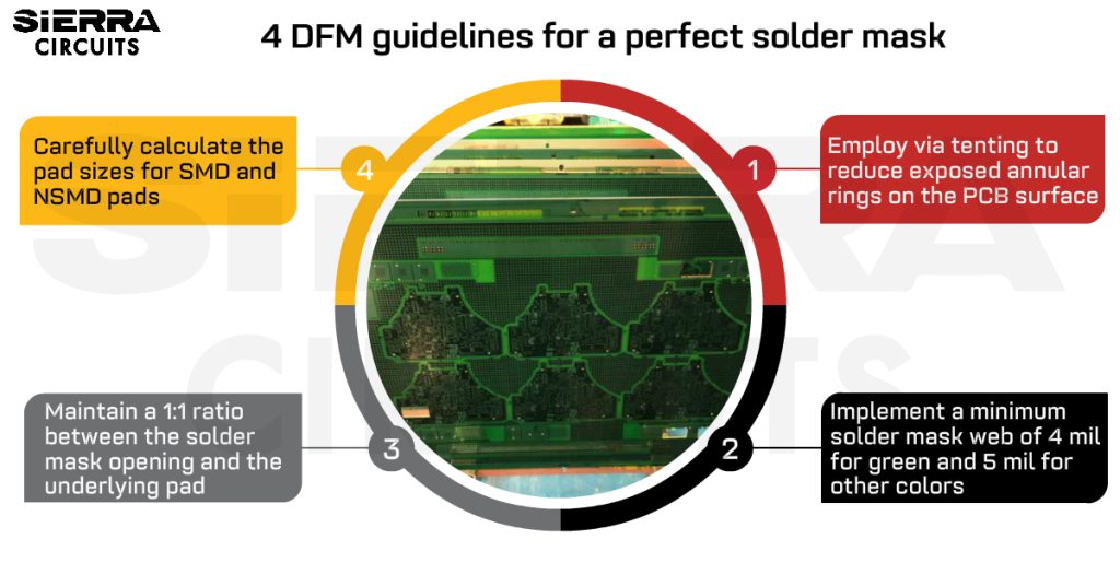
For defect-free assembly, adhere to these four solder mask/solder resist DFM rules: tent vias to prevent bridging, maintain minimum web width for durability, use a 1:1 mask-to-pad ratio for accuracy, and define SMD/NSMD pads correctly for joint integrity.
These rules are critical because the solder resist serves the vital function of insulating copper traces to eliminate electrical shorts while protecting the board from oxidation, environmental damage, and soldering errors.
Highlights:
- Solder mask layers protect circuit boards from oxidation, shorts, and environmental damage, ensuring optimal functionality.
- Inappropriate solder resist can cause issues like tombstones, solder balls, misalignment of components, and compromised soldering quality.
- Employ via tenting to prevent solder bridging and protect vias from the environment.
- Maintain a minimum solder mask web of 4 mil for green and 5 mil for other colors to ensure durability.
- Apply a 1:1 mask-to-pad opening ratio as the standard for optimal soldering and corrosion prevention.
- Correctly define SMD and NSMD pads to control solder joint formation and ensure reliability.
In this article, you will learn the solder mask layer types and DFM guidelines to design reliable, manufacturable PCBs.
What is a solder mask layer, and why use it?
Solder mask or resist is a protective layer that insulates the conductive traces and shields them from environmental contaminants such as moisture and dust. It typically comes in green. However, other colors, such as red, blue, and white, are also available.
Here’s a photograph of a PCB panel coated with a green mask.

The solder mask delivers these critical benefits across five key areas:
1. Provides insulation during the soldering process
A mask is an essential aspect of streamlining your circuit board assembly process. It effectively covers the entire board area where the components are not soldered. This ensures the components are placed in the intended locations.
2. Protects from corrosion and oxidation
Copper reacts when exposed to moisture and oxygen, losing electrons and changing its properties. While it retains its structural integrity when oxidized, its electrical properties are lost. Since PCBs rely on copper’s electrical characteristics, this is a major issue. As a result, a solder resist serves as the primary protective layer for your PCB by preventing corrosion and oxidation.
3. Prevents the growth of whiskers
Whiskers are thin filaments popping out of the circuit board. It leads to short circuits and hampers the board’s functionality. The presence of a mask can stop the growth of whiskers.
4. Strengthens the pads
The solder-resist layer reinforces the copper pads on the board’s surface area. It prevents pad separation from the PCB. This safeguard is crucial to ensure the structural integrity of your circuit board, especially in the case of flex PCBs.
5. Increases the breakdown voltage of the dielectric material
Breakdown voltage is the maximum voltage a PCB material can withstand without breaking down. The resist layer is made of a dielectric material. Placing it on a circuit board increases the breakdown voltage of the dielectric layer.
Click here to know more about other PCB surface layers.
4 DFM guidelines for solder mask design
Following key design-for-manufacturability guidelines for the solder mask ensures reliability and prevents assembly defects. Solder mask design requires fulfillment of certain criteria to avoid circuit board mask layer defects. Consider these tips for an error-free solder mask coating:
1. Employ via tenting to reduce exposed annular rings on the PCB surface
When a via is covered with solder mask coating so that it is not exposed, it’s called a tented via. Unlike via filling, here only the annular ring is covered by the solder mask. If the hole is closed completely, it is known as a filled via or mask-plugged via, depending on the method used to close the hole.
Tenting vias is a popular process used to protect PCBs and is chosen over epoxy filling or mask plugging due to cost considerations. Within methods of via tenting, liquid photo imageable (LPI) solder mask tenting is the most cost-effective. To ensure a better finish, you can also use resin filling, which is higher in cost.

The purpose of via tenting is to leave fewer exposed conductive pads on the PCB surface. This would minimize the shorts during solder bridging in the assembly process. It also reduces paste migration from SMT pads. It can happen when vias are on pad edges or in standard BGA dog-bone patterns. Tenting also minimizes the likelihood of a via being damaged through exposure to the operating environment.
2. Implement a minimum solder mask web of 4 mil for green and 5 mil for other colors
Solder mask web is an area of solder resist material adjacent to the mask openings. The mask web width should be 4 mil for green and 5 mil for other colors.

Also, incorporate a minimum of 1 mil solder mask coverage to avoid unintended electrical connections between traces.

3. Maintain a 1:1 ratio between the solder mask opening and the underlying pad
The outer layers of the PCB without the mask are solder mask openings. Its purpose is to expose the circuit to tin (solder). This opening has to be accurate, or it might lead to unnecessary exposure of copper on the board, leading to corrosion and damage.

Typically, fabricators choose to have solder mask openings 1:1 with the copper pads that can be altered to the appropriate manufacturing process. The opening can be customized based on your requirements.
In addition to this, always look for partially or completely missing solder mask layers. This can typically occur when you have complex geometries, such as acute angles.
4. Carefully calculate the pad sizes for SMD and NSMD pads
Solder mask-defined pads are those where the mask opening is smaller than the copper pad. Here, the solder mask coating will define the pad size used in BGAs. Thus, mask openings play a crucial role in deciding the pad size.

Non-solder mask-defined pads include a gap between the pad and the mask.
In the case of non-SMD pads, the mask openings and pad size are typically equal. Hence, you need to align the solder resist accurately with the pad edges. This is required to keep the whole pad free of solder masks and ensure optimal soldering per the new H revisions.
To learn more about SMD and NSMD pads, read solder mask-defined pads vs. non-solder mask-defined pads.

What are the types of solder mask?
PCB solder resists are available in four main types: top/bottom masks, epoxy liquid, liquid photoimageable (LPI), and dry film photoimageable.
The selection depends on the manufacturing process, performance needs (thermal stability, chemical resistance, electrical insulation), cost, and the PCB’s physical and environmental requirements, ensuring reliability and functionality for the intended application. In this section, we will have a look at different types of solder resists.
1. Top and bottom masks
These are typically used to identify openings in the green solder resist, which is already applied on the PCB. This particular layer of the mask is added through epoxy or film methods. Next, the component pins are soldered to the board utilizing the openings that have been registered using the masks.
The traces on the top side of the board are called top traces, and the corresponding solder mask used is called a top-side mask. Identical to the top-side mask, the bottom mask is used for the bottom side of the board.
2. Epoxy liquid solder masks
The most cost-effective option among solder resists is epoxy. It is a polymer that is silkscreened on the PCB. Silkscreening refers to a printing technique that uses a woven mesh to support ink-blocking patterns. The mesh enables the open areas to be identified for ink transfer. This step is then followed by thermal curing.
3. Liquid photoimageable solder masks
LPI masks are a mix of two distinct liquids. These liquids are kept separately and mixed right before applying the mask layer to enable longer shelf life. LPI is also one of the more cost-effective options among various other types.
LPI resist is employed for curtain coating, screen printing, and spray applications. This mask is a blend of various polymers and solvents. A thin coating can be formed using this mask that can stick to the target area’s surface.
Unlike conventional epoxy inks, LPI is sensitive to UV light. The panel must be covered with the mask, and after a short tack cure cycle, the board is exposed to UV light using a UV laser or photolithography process.
Before mask application, the panels are subjected to cleaning and are checked for any signs of oxidation. This is done using a chemical solution, aluminum oxide solution, or suspended pumice to scrub the panels.
One of the most popular techniques used to expose the panel surface to UV light is through the use of film tools and contact printers. The top and bottom sheets of the film are printed using emulsion to block areas that need to be soldered. Production panels and film are then fixed in position, using tooling on the printer, and exposed to a UV light source simultaneously.
One method utilizes direct imaging that makes use of a laser. This technique does not need tooling or film, as the laser is controlled through fiducial markers placed on the copper template of the panel.
4. Dry film photoimageable solder resists
The use of dry film photoimageable solder masks requires vacuum lamination. This dry film is subjected to exposure and then developed. Post-development, openings are identified to generate a pattern, after which the components are soldered to the copper pads. High-density wiring boards benefit most from dry film masks as they do not flood the through-holes.
For more DFM guidelines, download the Design for Manufacturing Handbook.

Design for Manufacturing Handbook
11 Chapters - 96 Pages - 90 Minute ReadWhat's Inside:
- Annular rings: avoid drill breakouts
- Vias: optimize your design
- Trace width and space: follow the best practices
- Solder mask and silkscreen: get the must-knows
Download Now
What is the standard thickness of a solder mask layer?
Standard solder mask thickness is at least 0.8 mil perpendicular to the board. The thickness over a circuit’s corner may be as thin as 0.3 mil.
It is recommended to have approximately 0.5 mil of mask covering on your board for balanced protection and soldering performance.
If the mask is too thin, it may result in copper exposure, leading to potential SMT issues.
If the mask is too thick, it leads to misalignment of components, compromising the soldering quality. Furthermore, thick resists can make it harder for the solder to flow well during reflow soldering, causing solder balls to form.
What are the different solder mask colors used in PCBs?
Green is the most common solder mask color due to tradition and good contrast, but red, blue, black, white, yellow, and purple are available for visibility, branding, or inspection needs.
The table below lists the colors in which masks are available.
| Solder mask color | Features |
|---|---|
| Green | The most common resist color. It offers the highest resolution due to its superior UV light absorption capability |
| Red/blue | Have a resolution similar to green solder masks |
| Black | Offers the lowest contrast between the board and the traces, which makes visibility and inspection difficult |
| White | Rarely used due to poor visibility, and are usually ideal for LED applications |
| Transparent | Provides a superior level of detail and resolution |
The conventional choice for solder resists is typically green; however, an increasing variety of shades have become available to accommodate design requirements. These requirements include a product classification system, the differentiation of prototype runs and revision changes, and the aesthetic enhancement of boards.

IPC-SM-840 standards for solder masks
IPC-SM-840 defines qualification and performance requirements for solder mask materials, classifying them into telecommunications (T/FT) and high-reliability/military (H/FH) categories with specific tests for adhesion, hardness, flammability, and environmental resistance.
The intended application of solder mask coating is defined in the categories below:
T – telecommunication
This category comprises telecommunication devices, computers, and equipment in non-critical military applications. Solder mask coating and coverlay on boards in this class are suited to high-performance industrial and commercial products. Such products require extended performance life, but interrupted service would not result in life-threatening situations.
H – high reliability/military
This consists of equipment where progressive performance requirements are critical, and device downtime is unacceptable. Solder mask coating and coverlay on boards of this PCB class are meant for applications that are critical, and uninterrupted service is completely essential.
FT – flexible printed board applications (telecommunications)
This is applicable to cover materials that are used for flexible board applications in telecommunications equipment.
FH – flexible printed board applications (high reliability/military)
This is applicable to cover materials that are utilized for flexible PCB applications that are required in military applications, which call for high-reliability requirements.
Flexible cover materials have been appended to revision “E” of the IPC standards. Solder mask coating material requirements fit into three IPC classes of bare boards:
- Class 1 PCBs that don’t require solder mask coating
- Class 2 boards that fit the class T/FT (telecommunications) mask needs
- Class 3 circuit boards that match class H/FH (high-reliability military) mask requirements
The mask requirements mentioned above are meant to state parameters such as hardness, shelf life, flammability, and board adhesion. It also states the resistance to soldering, biological growth, moisture, and chemicals such as fluxes, cleaning agents, and solvents.
Another important consideration is choosing a matte or satin finish over a gloss or semi-gloss finish. It helps minimize solder beading and reduces glare during manual processes and inspection. Procurement documents or fabrication drawings usually specify if there is conformance to IPC-6012 standards. When this standard is stated for conformance, the solder mask coating is covered by IPC-6012 section 3.7.
For more, download the IPC Standards Handbook.

IPC Class 3 Design Guide
8 Chapters - 23 Pages - 35 Minute ReadWhat's Inside:
- IPC guidelines for manufacturing defects
- IPC standards for assembly processes
- Common differences between the classes
- IPC documents to set the level of acceptance criteria
Download Now
How is solder mask applied to circuit boards?
Solder mask is typically applied through a multi-step photolithographic process involving cleaning, ink coating, pre-hardening, UV imaging, developing, and final curing, or via modern inkjet direct printing for simpler, eco-friendly application.

The conventional process applies a solder mask using photolithography to precisely define openings, ensuring consistent coverage and alignment with copper features. Here is the step-by-step of the solder resist application process:
Step 1: Board cleaning
The board is cleaned to remove dirt and other contaminants, and the board surface is dried.
Step 2: Solder mask ink coating
Next, the board is loaded into a vertical coater for solder mask ink coating. Coating thickness is decided by factors such as the reliability required for the PCB and the environment in which it will be used. The mask thickness varies depending on which section of the board it is added to (traces, planes, substrate). It also depends on your CM’s PCB manufacturing capabilities.
Step 3: Pre-hardening
This facilitates the removal of the unwanted coating, which can be easily removed from the PCB in the developing stage.
Step 4: Imaging and hardening
Imaging is done using a photo film, which is laser plotted to define the mask area. This film is aligned with the panel that is already solder ink-coated and tack-dried. During this imaging process, the film aligned to the panel is exposed to UV. Upon receiving the UV light, the opaque area allows the UV light to transfer through the film, and thereby, the ink below the opaque gets polymerized (hardened).
In the case of LDI imaging, the photo films are not required as the UV laser will directly harden the portions on the board that need to retain the mask ink.
Step 5: Developing
The circuit board is then dipped in the developer to clean away the unwanted solder resist to ensure the required copper foil is accurately exposed.
Step 6: Final hardening and cleaning
Final hardening is necessary to make the solder resist achieve the final hardening state. Next, the boards must be cleaned before further processes, such as PCB surface finish.
How is solder mask applied through inkjet technology?
Inkjet (or direct jetting) solder mask application uses piezoelectric print heads to deposit resist only where needed, eliminating film tools, reducing waste, and shortening the production cycle.
PCB manufacturing has predominantly used inkjet systems to create nomenclature markings in the last decade. In recent years, however, technology has evolved, enabling fabricators to print solder resist directly onto the board surface.
Compared to the method based on photolithography, the DJ method cuts down most of the process steps, leading to these advantages:
- Minimized material usage
- Reduced capital equipment and process variables
- Eco-friendly processing
- Elimination of excess use of solder resist
What is a peelable solder mask?
A peelable mask is a temporary resist that is sometimes used in the PCB assembly process to protect certain areas of the board. When the PCB assembly process is complete, the mask is removed mechanically or peeled off by hand. A peelable mask is not a replacement or substitute for a standard resist, but it’s a different entity altogether.

When should you use peelable solder resist?
Use peelable solder mask to protect unused pads, vias, or finish-sensitive areas during assembly or surface finishing, especially when manual rework or selective plating is required.
The main objective of the peelable solder resist is to protect the selected board surface during wave soldering, reflow soldering, hot-air solder leveling (HASL), or surface finish procedures.
Before PCB Assembly, a peelable mask is applied onto pads or plated through holes to prevent extra solder from building up on the empty pads.
You can use a peelable resist when you have a component that needs to be assembled manually. It can also be used to cover board surfaces that require selective surface finishes.
Difference between solder resist and paste mask
Solder resist is a permanent insulating polymer layer that covers non-solderable copper, while a paste mask (stencil) is a temporary steel or polymer tool used only during SMT assembly to apply solder paste to pads. The table below provides the key differences:
| Solder mask | Paste mask |
|---|---|
|
Protective polymer layer that exposes copper pads for soldering while covering other areas
|
Metal stencil pattern that defines where solder paste is deposited during assembly
|
|
Prevents solder bridging, short circuits, oxidation, and environmental damage
|
Enables precise and controlled application of solder paste onto pads
|
|
Applied during PCB fabrication
|
Used during PCB assembly (SMT process) |
| Made of dielectric material (e.g., epoxy, LPI) |
Made with thin stainless steel or nickel sheet (the stencil itself)
|

Key takeaways:
- Solder resist types include top and bottom masks, epoxy liquid masks, liquid photoimageable (LPI), and dry film photoimageable resists.
- The color of the resist does not affect the electrical properties, but it affects visibility, inspection, and aesthetics.
- Mask thickness is critical for PCB performance; too thin may expose copper, leading to SMT issues, while too thick can cause misalignment and soldering problems.
- The standard solder mask thickness is at least 0.8 mil, but it may vary depending on the specific location on the board. It is recommended to have approximately 0.5 mils of mask covering traces.
- Applying a solder resist onto a PCB involves board cleaning, ink coating, pre-hardening, imaging and hardening, developing, and final hardening and cleaning.
Need assistance in designing a solder resist on your circuit board? Post your queries on SierraConnect; we will be happy to help you.

About Mohamed Faheemuddin : Mohamed Faheemuddin is a mechanical engineer. His passion for electronics drew him to the PCB industry. With an experience of over 3 years in the PCB industry, he specializes in developing articles for engineers and hardware designers.