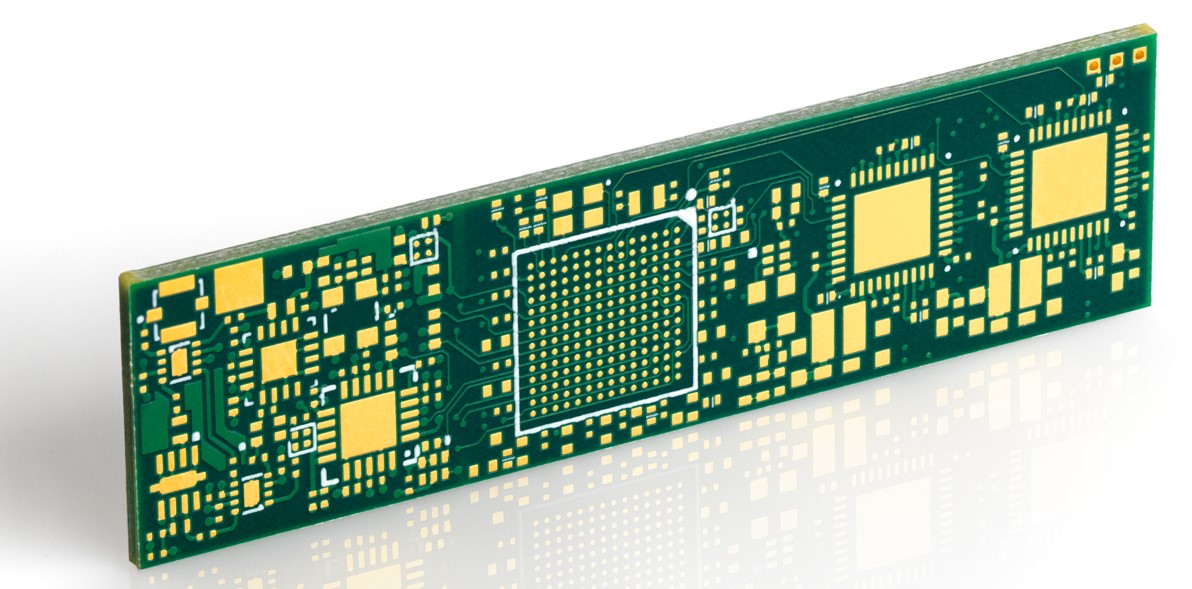
Hard gold is a type of surface finish applied to high wear areas, such as edge connectors, keyboards, or gold/edge fingers on PCBs. This finish provides a robust surface against depreciation.
What is hard gold surface finish on PCBs?
The hard gold finish basically offers tough resistance to friction compared to other finishes. It is used to create gold/edge fingers on circuit boards. This finish is the best option when a PCB is designed to be inserted into another board, such as RAM. Hard gold is extremely durable, thus can withstand repeated usage. This finish is expensive and has poor solderability, hence, it is not applied on solderable surfaces.
Whenever there is a requirement to plate specific areas on the board with hard gold, you can opt for selective gold plating. The process of selective gold plating is a bit different. For this reason, it is necessary to specify your requirements while raising a quotation.
Also, see types of circuit board surface finishes.
How hard is the applied gold finish?
The plating procedure uses gold because gold has high corrosion resistance, high electrical conductivity, and can be alloyed with cobalt or nickel to develop resistance to wear and tear. Gold plating can range in thickness from 3µ” to 50µ”.

Hard gold finish, also known as electrolytic hard gold, is made of a layer of gold with hardeners that will maximize durability. Using an electrolytic process, it is plated over a nickel barrier coating. The thickness of this plating varies according to the duration of the plating cycle. The minimum values for gold/edge fingers are given below:
| Gold | Nickel | Classes |
|---|---|---|
| 30 µ” | 100 µ” | Class 1 |
| 30 µ” | 100 µ” | Class 2 |
| 50 µ” | 100 µ” | Class 3 |

Connector Design Guide
5 Chapters - 32 Pages - 50 Minute ReadWhat's Inside:
- Basics
- Terminology
- Selection and layout rules
- Testing
- Application-specific PCB connectors
Download Now
Pros and cons of hard gold
The pros are listed below:
- Tough and durable surface
- Long service life
- No toxic elements like lead, hence environment-friendly.
The cons are:
- Expensive and poorly solderable
- More processing time
- Possibility of flaking due to undercut etching
- Problems with other finishes
Hard gold plating is commonly used for connector interfaces. Read our detailed guide on gold fingers to understand their design considerations, beveling requirements, and plating specifications.
Important properties of hard gold finish
While selecting a hard gold finish, consider the following critical aspects:
Bonding considerations
The soldering of hard gold deposits is challenging due to the presence of non-noble elements like nickel, cobalt, etc. These metals oxidize at soldering temperatures and reduce the strength of the solder joint. Hence, this finish is not suitable for any kind of joining process.
For applications such as ultrasonic wire bonding, thermosonic bonding, etc. ENIG is preferred. The thickness and purity of gold are ideal for these processes.
Apperance
The appearance of hard gold plating is bright because of its refined grain structure. In light of this impression, it is an excellent choice for applications requiring cosmetically pleasing gold contacts, such as visible interconnect applications.
Corrosion resistance
Gold finish minimizes the corrosion resistance of the coating due to the added non-noble elements. It is easily oxidized at elevated temperatures.
Wear resistance
This finish consists of metallic elements like nickel, iron, or cobalt. Due to these elements, deposits develop finer grain structures that are more lustrous and resist sliding wear.
These are some factors that will help you determine the appropriate surface finish.


