


Contents

On-demand webinar
How Good is My Shield? An Introduction to Transfer Impedance and Shielding Effectiveness
by Karen Burnham
A bill of materials (BOM) is a document that lists all the components required to assemble a printed circuit board (PCB), along with details such as quantities, part numbers, reference designators, and sourcing information.
As a PCB designer or procurement engineer, understanding BOM requirements can help you avoid sourcing delays, assembly errors, and costly design revisions while ensuring a smooth transition from design to production.
In this article, we explain what a PCB bill of materials is, the information it should contain, its role in the assembly process, and how to create one using ECAD tools.
Highlights:
- Essential BOM fields include part quantities, manufacturer part numbers (MPNs), reference designators, footprints, and sourcing details.
- BOM tools can validate component availability, compare vendor pricing, and suggest alternate parts when components are out of stock.
- Modern ECAD tools can automatically generate BOMs from PCB schematics, simplifying documentation and procurement.
What is a BOM?
A BOM is a detailed list of all the components, materials, and parts required to manufacture a product. It is typically stored in a BOM file and serves as a critical reference throughout the production process. Manufacturers rely on the BOM to ensure accurate planning, procurement, assembly, and quality control.

Customers can also use the bill of materials to communicate their assembly requirements clearly, helping fabricators understand exactly which components are needed to build the product.
The example below shows a customer checklist, and we can see that the BOM is one of the many important documents submitted by the customer to a PCB manufacturer.

The BOM lists all the components required for a given number of boards. An example is given below.

To learn how to avoid assembly delays, download the Design for Assembly Handbook.

PCB Design for Assembly Handbook
6 Chapters - 50 Pages - 70 Minute ReadWhat's Inside:
- Recommended layout for components
- Common PCB assembly defects
- Factors that impact the cost of the PCB assembly, including:
- Component packages
- Board assembly volumes
Download Now
What is the purpose of the bill of materials?
A well-structured BOM is required to improve efficiency across the PCB development process. It centralizes the component data, simplifies procurement, and supports accurate cost estimation.

Single source of component data
During the PCB assembly process, a BOM acts as a single source to provide information about all the components. It includes critical details such as quantities, reference designators, footprints, manufacturer part numbers, and sourcing information. By consolidating all component data into one document, teams can improve coordination, reduce errors, and streamline the design and manufacturing process.
To streamline component validation and pricing analysis, we recommend using Sierra Circuits’ standard BOM format when preparing your file.
Download our preferred BOM format.
If the BOM is properly updated, then there will not be any chances of redesign during the later stages. Hence, an updated BOM saves time and effort.
Are you worried about sourcing low-quality/counterfeit components, price inflation, and inefficient inventory management? We got you covered. Sierra Circuits’ customer-owned inventory services (COIN) is a personalized component sourcing and stocking program designed to meet your specific needs.
With COIN, we procure and store the required parts for your PCBAs, eliminating the risk of counterfeit or low-quality components while ensuring you have access to the necessary parts when you need them.
See our FAQs on COIN services.
Easier cost estimation and procurement
Cost estimation is a major decision when it comes to PCB projects. By understanding the cost drivers for circuit boards, designers can better manage budgets and optimize their designs for manufacturability.
When the designers are in the initial stages of figuring out how many boards they need and the parts required for those boards, a BOM list can be really helpful.
Now, most of the time, designers have a tough time meeting the target cost of the whole project. Analyzing their BOMs, they can figure out the availability and cost of different components. Hence, they can alter their design in the initial stages as required to fit in the target cost range.
Most of the PCB manufacturers these days offer BOM tools that run this cost estimation check with different vendors. These tools compare the parts mentioned in the list with the real-time stocks available with their specified vendors.
BOM tools also let the designer know whether a certain part is available for purchase or not. If not, alternate part numbers with the same specifications will be suggested. The discounted prices are considered when it comes to bulk ordering of components. Hence, these tools are very helpful for cost estimation.

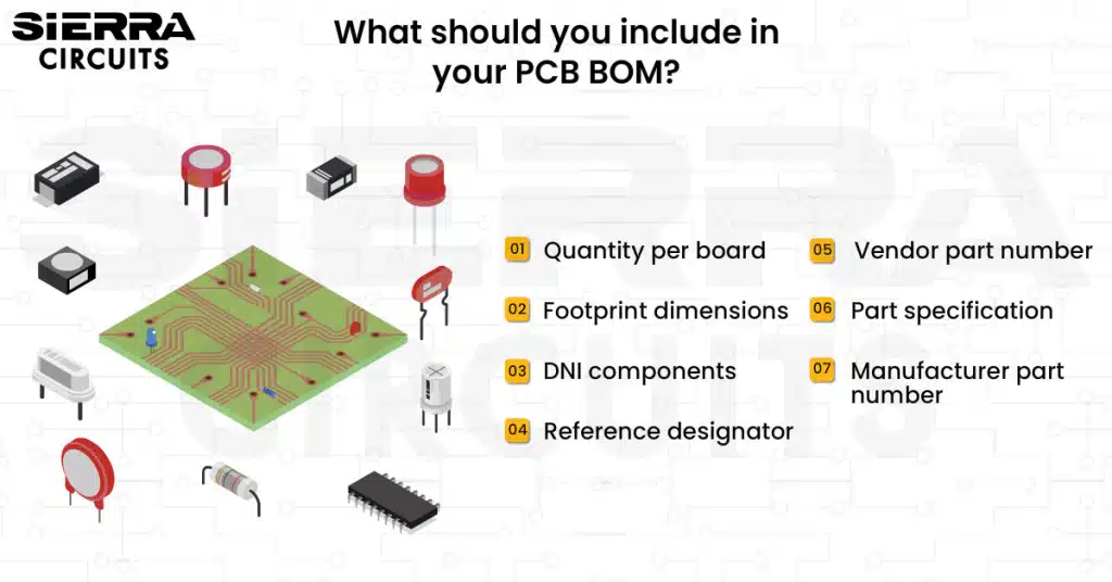
What to include in your bill of materials for a PCB?
A BOM should include component descriptions, part numbers, quantities, reference designators, package/footprint details, manufacturer and vendor information, assembly instructions, and sourcing data to ensure accurate procurement and production.
The following are the fields required in any BOM, irrespective of the PCB manufacturer:
- Item: Gives the index for all the specifications mentioned in the BOM.
- Quantity per board: Specifies the quantity of a particular part to be used in each board.
- Manufacturer part number (MPN): Helps to identify the part easily throughout the process.
- Do not install (DNI): This field indicates whether the components should be populated or not to be populated on the board.
- Reference designator of components: Eliminates any confusion regarding the position of a particular part on the layout of the board, as each part will have a specific reference designator.
- Vendor (optional): Name of the vendor.
- Vendor part number (VPN) (optional): Part number designated by the vendor.
- Value (optional): Value of the particular part.
- Size/footprint: The size/footprint of each part number helps to understand the amount of space it is going to accommodate in the PCB layout.
- Part description/specs (recommended): This is the field where designers can add the specifications of each part.
- Manufacturer (optional): Name of the part manufacturer.
Read our case study, eliminating BOM and footprint errors in PCB assembly, to see how we resolved material list issues to achieve an error-free board.
Need assistance with component sourcing and cost optimization?
You can book a meeting with our experts or call us at +1 (800) 763-7503.
How to create a bill of materials?
A BOM can be created simply by using a spreadsheet and entering the list of parts required. This is a tedious process that consumes so much time and effort. But with the advancement of technology, now there are means of creating BOMs that are updated as per the part availability. This is the reason why designers now opt for software tools to create the bill of materials.
During the electronic circuit design phase, the BOM is generated from the schematic ECAD tool.

Using these ECAD tools, designers can first draw a PCB schematic. These tools will have information regarding the part numbers in the library. When designers add each part to the schematic, the part information is also pulled from this library. ECAD tools use the same information for creating the bill of materials for that specific schematic.
Among the available software, the most commonly used are Altium Designer, Allegro PCB editor, KiCad, and many more.
Once BOM files are created, they help designers in the following:
- Total cost: Using a BOM, PCB designers can understand the total cost for the number of boards to be assembled.
- Availability of the parts: The parts that are chosen should be in stock. After generating the bill of materials, the stocks of the required components can be checked.
- Life cycle: The parts to be ordered should have an active lifecycle.
- Bulk ordering price: When ordered in bulk quantities, some vendors offer a discounted price. Since BOMs have all the parts required, bulk orders can be placed.
- Easy format change: The format of generated BOMs can be changed easily. This gives the option to send BOMs in any format required by the fabricators.
The importance of having a BOM with all the required components with their specifications is very clear now. Therefore, designers should first have a look at the template offered by the PCB manufacturer. After this, they can generate the bill of materials in the specified format and use a BOM tool to check it and get a quote.
Have queries on designing your next boards? Post them on our community, SierraConnect. Our design experts will answer them.


