Design rule check (DRC) verifies that your layout complies with the constraints defined in your EDA tool, while design for manufacturability (DFM) evaluates whether your PCB can be fabricated reliably.
Understanding the difference between DRC and DFM helps PCB engineers avoid expensive re-spins, improve yield, and move prototypes into production more efficiently.
In this article, we break down DRC and DFM and explain why considering both throughout the layout development cycle is important.
Highlights:
- DRC identifies layout violations like trace spacing issues, undersized vias, and inadequate annular rings.
- Design for manufacturing verifies whether board features align with your contract manufacturer’s (CM) fabrication capabilities.
- Run DFM tests at schematic, placement, routing, and final layout stages.
What DRC validates in your PCB layout
Design rule check verifies whether a circuit board layout follows a predefined set of rules. They include minimum trace width and spacing, length tuning, teardrops, and custom rules. These constraints are typically derived from IPC standards (IPC-6012, IPC-2221, IPC-7351).
The results are generally binary (pass/fail). Correct any errors before proceeding to the next phase. DRC ensures consistency and adherence to layout constraints; it does not account for process variations or manufacturing tolerances.
When should engineers run a design rule check?
Run this test throughout the development process, especially before finalizing the layout. It looks for violations such as:
- Insufficient trace width and spacing
- Undersized vias
- Copper feature clearance errors
If you haven’t finalized your fabricator, define the rules based on the industry standards. Once a manufacturer is selected, update the constraints to reflect their specific capabilities, tolerances, and process limits.
Always review the manufacturer’s capabilities before running a DRC, as this ensures your constraints align with real fabrication limits.
For more, see how to run a design rule check (DRC) for your PCBs.
What DFM evaluates
Design for manufacturing evaluates whether a board can be fabricated reliably and cost-effectively. It is manufacturing-focused and ensures that the layout is optimized for volume production.
Unlike DRC, DFM goes beyond strict rule checking and analyzes process sensitivity and manufacturing risk, capabilities, and tolerances. A layout may pass DRC but still present challenges during production.
Design for manufacturing rules consider factors such as:
Instead of only flagging errors, it highlights the potential DFM issues.
What are the differences between DRC and DFM?
Design rule check verifies that a board layout adheres to all the predefined constraints set by the design engineer, such as trace widths, clearances, and via sizes, configured within the EDA tool for automated validation.
Design for manufacturing, on the other hand, evaluates whether the prototype can be reliably produced within the capabilities and tolerances of the board manufacturer.
The infographic below (DRC vs. DFM) highlights these differences across key parameters.

A common misconception is that passing DRC guarantees the layout is ready for manufacturing. In reality, a PCB can pass design rule check and still fail in production.
For example, a printed board via may meet the minimum annular ring requirement set in the EDA tool, but DFM analysis might flag it as high risk due to drill misalignment tolerances, potentially leading to open circuits during fabrication.
This is why relying solely on design rule check can create a false sense of security, often resulting in board respins, engineering change orders (ECOs), project delays, and increased costs.
Sierra Circuits fabricates and assembles high-quality PCBs using cutting-edge technologies such as X-ray drill machines, mechanical vision drilling systems, and Seica flying probe test machines.
Visit our rigid PCB manufacturing capabilities to learn more.
When should engineers perform DFM checks?
It is often assumed that DFM is solely the manufacturer’s responsibility, but designers should also perform it continuously throughout the development phase.

Recommended stages:
- Schematic
- Validate component footprints
- Ensure part availability and suitability
- Component placement
- Check spacing for assembly
- Evaluate heat dissipation techniques
- Routing
- Analyze vias and aspect ratios
- Review impedance and copper distribution
- Final layout approval
- Perform full validation
- Prepare for circuit board fabrication and panelization
Oren Manor, Director of Siemens EDA Business, explained: “You don’t need to run every single DFM check at every stage of the layout. Instead, focus on 10-20 relevant checks at each stage. This way, you detect and fix issues early, and changes are still quick and inexpensive to make.”
To learn how to align your layout with the manufacturer’s capability, watch our webinar: designing for manufacturing from PCB stack-up to assembly success.
When do manufacturers perform design for manufacturing analysis?
Once fabricators receive the design files, they perform a comprehensive DFM analysis to ensure the board can be manufactured reliably. This stage typically occurs before production begins and focuses on validating the layout against the fab house’s capabilities.
Manufacturers evaluate fabrication tolerances, drilling constraints, material compatibility, panelization, and assembly requirements to minimize production risks and improve yield.
Typical DFM checks include:
- Pre-production review of Gerber/ODB++/IPC-2581
- IPC manufacturing standards (class 2/class 3)
- Stack-up and board features
- Fabrication feasibility analysis (etching, plating, and drilling limits)
- Via filling, solder mask, and silkscreen requirements
- Panelization and yield optimization
- Annular ring issues, slivers, drill misalignment, and mask coverage problems
At Sierra Circuits, we perform thorough DFM analysis to avoid potential board defects.
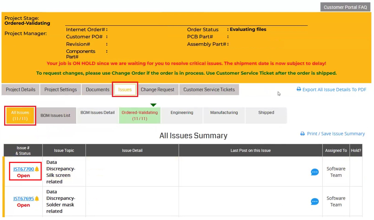
Our engineers will raise issue tickets (ISTs) for any DFM errors identified during the design review. You can track and resolve these through the Sierra Circuits’ customer portal.
To learn more, talk to a PCB expert: Book a meeting or call us at +1 (800) 763-7503.
A clear understanding of DRC vs. DFM aspects is important to reduce the risk of respins, production delays, and yield loss. Collaborate with your manufacturer early to ensure that your prototype aligns with actual fabrication capabilities, not just theoretical limits.
For DFM strategies, download the Design for Manufacturing Handbook.

Design for Manufacturing Handbook
11 Chapters - 96 Pages - 90 Minute ReadWhat's Inside:
- Annular rings: avoid drill breakouts
- Vias: optimize your design
- Trace width and space: follow the best practices
- Solder mask and silkscreen: get the must-knows


