


Contents

On-demand webinar
How Good is My Shield? An Introduction to Transfer Impedance and Shielding Effectiveness
by Karen Burnham
Every PCB should be designed in such a way that the overall cost and chances of potential DFM (design for manufacturability) issues can be minimized. It is a process of arranging the PCB layout to resolve problems that may arise during fabrication and assembly.
DFM checks each design before the files go for fabrication. It will point out the potential defects in advance and ensure the boards are manufactured to the exact specifications.
Highlights:
- Run DFM checks iteratively throughout the design stages to avoid respins.
- Check for common errors like insufficient annular rings and clearances before submitting your design files.
- Maintain adequate drill-to-copper clearance and aspect ratios to ensure manufacturability.
In this blog, you’ll learn the importance of design for manufacturing, 5 common DFM issues to watch out for, and techniques to avoid them.
What is design for manufacturability in a PCB?
DFM is a set of design guidelines that helps you ensure your boards can be easily manufactured.
By following the design for manufacturing rules, you can:
- Reduce production costs.
- Improve product reliability.
- Accelerate time-to-market.
Consider these DFM parameters before finalizing your design:

When you run a DFM check, you get:
- Visual representation of DFM errors: As a layout engineer, you can interactively review DFM issues one by one. This helps you understand and fix violations before finalizing the design.
- Comprehensive DFM report: At the end of the process, you receive an auto-generated, detailed report that is:
- Shareable with teammates, consultants, or manufacturers
- Archivable as a part of your design documentation
This approach is often called manufacturing-driven design.

6 common misconceptions about design for manufacturability
- DFM is the sole responsibility of the manufacturer.
- DFM and DRC are essentially the same.
- Defining PCB design for manufacturing rules is overly complex and time-consuming.
- Running DFM requires specialized knowledge across multiple tools.
- It can be deferred until the end of the design process.
- It is only relevant for large enterprises with high-volume production.
Who should perform DFM checks for PCB designs?
Design for manufacturability is often considered solely as the manufacturer’s responsibility. However, according to Oren Manor, Director of Siemens EDA Business, both designers and manufacturers should be involved in DFM checks.
The table below highlights how DFM checks benefit manufacturers and designers.
| Manufacturers’ benefits | Designers’ benefits |
|---|---|
|
|
Running DFM early helps make sure your PCB design matches the manufacturer’s capabilities, reducing the risk of fabrication defects.
Design for manufacturing vs. design rule check
It’s important to distinguish design for manufacturing from design rule check (DRC), as they serve different purposes:
What DRC does
DRC verifies if your design meets a set of predefined rules, usually defined by the industry standards. It flags violations like insufficient trace spacing and undersized vias. DRC ensures consistency and good design practices across the board. However, it doesn’t consider the actual manufacturing capabilities.
What DFM does
Design for manufacturing checks whether your board can be fabricated and assembled efficiently. Unlike DRC, it doesn’t just flag critical errors. It also highlights yellow zone warnings. These errors may technically pass DRC but could still cause problems, such as lower production yields, higher manufacturing costs, and long-term reliability issues.
For a better understanding, let’s look at how DRC and DFM differ in terms of annular ring and drill-to-copper spacing in the table below:
| Parameter | DRC | DFM |
|---|---|---|
| Annular ring | Uses a minimum allowed annular ring value | Analyzes ring size based on manufacturing process (e.g., laser-drilled via, mechanically drilled through-hole, backdrill) |
| Drill-to-copper spacing | Checks basic spacing requirements between the drill and the copper | Adjusts spacing rules based on process type; PTH may allow tighter spacing than NPTH |
For more, see design rule check vs. design for manufacturing.
When should you run a DFM check?
Generally, DFM analysis is performed at the end of the design phase. However, late checks can lead to issues such as internal engineering change orders (ECOs), board respins, delays, and an added cost.
Instead of waiting until the end, DFM checks should be performed at different stages of the design process, such as:
- Schematic
- Component placement
- Routing
- Final layout approval
A practical approach is to run targeted design for manufacturing checks (10-20 at a time) at each stage rather than all checks at once. This helps catch issues early, when they are easier and cheaper to fix.
These tests can slightly increase your design costs. However, this small investment saves money in the long run by ensuring manufacturability and avoiding common manufacturing errors.
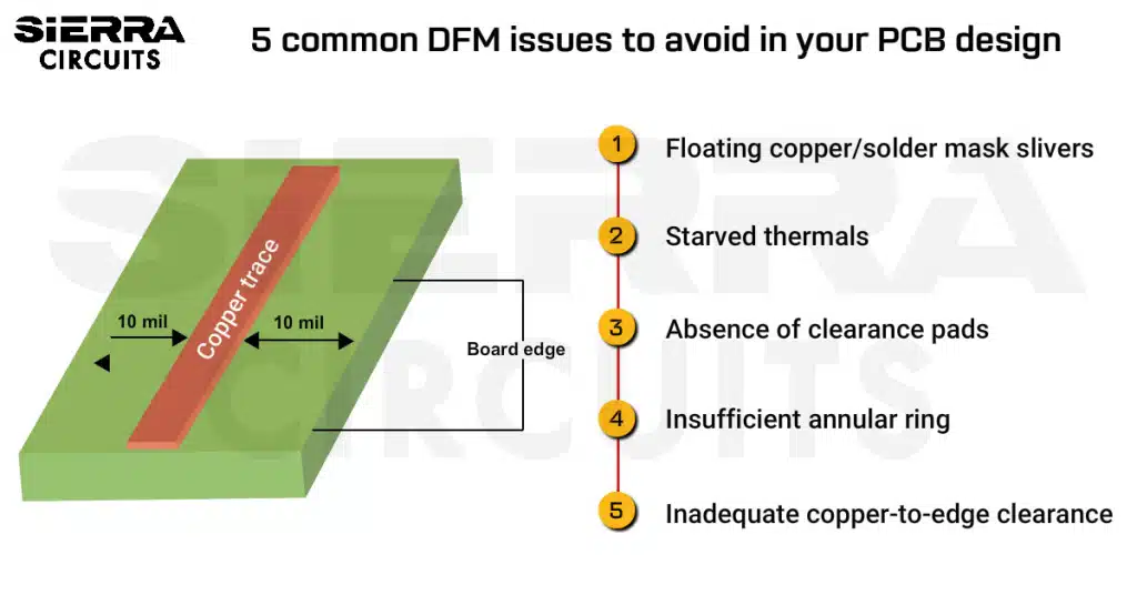
5 common DFM issues to avoid in your PCB design
Avoiding DFM issues is a better approach than letting them ruin your circuit design and then looking for a remedy. Checking for manufacturability is a smart move from your side. It solves problems before they appear. The issues in the design can be due to:
- Non-functional circuit layout.
- Board functions but not as intended (within the specification). It happens due to component mismatch and timing errors in a board.
- Random failure that does not reflect any connection with the possible situation.
Keeping track of design rules and performing consistent checks can help you avoid the following DFM issues:
1. Floating copper/solder mask slivers create antennas
Slivers are small, free-floating wedges of copper (conductive) or solder mask (non-conductive) on the plane. These can get redeposited to other copper pieces or exposed copper to create shorts.
If they are big enough not to float, then they form an antenna, responsible for noise and other interferences within the board. Now, the question is, why do they create an antenna? Because they have no grounding, they act as a signal catcher.

How to avoid copper slivers? Slivers can be avoided by maintaining copper features around 0.004 inches. In the example given below, we are talking about the spacing between antipads.
This trick is not 100% foolproof, but it greatly reduces the chances of copper redeposition elsewhere on the layer. This depends on the copper weight. The higher the copper weight, the wider the connection area required.

To learn about prevalent solder resist defects, see 6 common solder mask errors every PCB designer should know.
2. Starved thermals cause soldering issues
Thermals are the small copper spokes in a thermal relief pad, used to provide sufficient heat for the soldering process. The spokes prevent the heat from dissipating, which helps create a robust solder joint and an accurate electrical connection between the pad and the plane.
In some cases, voids between the thermal and the plane or the pad can lead to an incomplete connection, minimizing the heat concentration required to form a proper joint. This, in turn, can lead to various functional problems.
Such thermals affected by voids are called starved thermals. This may solder irregularly or take a longer time to reflow during the assembly process.

Thermal performance directly affects board reliability. Follow these techniques to efficiently dissipate heat in high-power designs:
- Use thicker copper (e.g., 3 oz/ft² or 4 oz/ft²) for power planes to improve heat spreading.
- Add vias under high-power components (e.g., power ICs) to transfer heat to the inner or bottom layers.
- Use copper pours for better heat distribution. Ensure at least 7 mil spacing between copper pour and adjacent traces.
- Place thermal pads under components to enhance heat transfer to the PCB.
- Route high-power traces on outer layers for better airflow or heatsink attachment.
- Provide sufficient air ventilation over heat sinks for effective heat dissipation.

Ventilation channels help dissipate heat from a PCB.
If your design includes thermal vias in ground slugs, discuss with your CM whether to cap or plug them based on their manufacturing capabilities. This early alignment ensures thermal reliability without causing delays during fabrication.
For more heat dissipation techniques, see 12 PCB thermal management techniques to reduce heating.
3. Absence of a clearance pad causes shorts
Pins (plated through holes) that are missing a clearance pad will connect to a plane layer. If clearance pads are unavailable from all plane layers for the pin, it will connect all of the voltage planes.
4. Insufficient annular ring results in an open circuit
Drill size is specified that exceeds the annular ring size being drilled, and can result in a disconnect of the pin or a short in a voltage plane.

5. Copper too close to the board edge causes shorts in adjacent layers
Sometimes, insufficient clearance is provided between the copper and the PCB edge. If copper is too close to the edge, then shorts can be created when current is applied to the panel between the adjacent layers. It happens due to the exposed copper around the perimeter of the board.
Design tip: DFM issues can be avoided by following DRCs for DFM checks.

Design for Manufacturing Handbook
11 Chapters - 96 Pages - 90 Minute ReadWhat's Inside:
- Annular rings: avoid drill breakouts
- Vias: optimize your design
- Trace width and space: follow the best practices
- Solder mask and silkscreen: get the must-knows
Download Now
Checks for controlling DFM issues
DFM checks are mandatory for designing a PCB with optimum manufacturability. This can save you from the disastrous effects of potential defects.
1. Avoiding DFM violations in drilled holes
The hole drilling process is the foundation for vias and the connectivity between different layers. It is the most expensive, irreversible, and time-consuming step in the PCB manufacturing process.
As soon as the number of holes increases, the check for drill-to-copper spacing becomes critical. Two significant aspects to be considered in the drilling process: aspect ratio and drill-to-copper clearance (drill to the nearest copper feature).

1.1 Aspect ratio (AR): The ideal aspect ratio is 10:1 for through holes and 0.75:1 for microvias. When the aspect ratio is larger, it becomes more difficult to achieve reliable copper plating inside the vias.
It will also add to the time for manufacturing and cost. Hence, the smaller the aspect ratio, the higher the PCB reliability. At Sierra Circuits, we offer an aspect ratio of 0.75:1 for microvias.
AR (Through-Hole) = [(Thickness of the PCB) / (Smallest drilled hole)]
Since microvias don’t protrude through the entire board, the aspect ratio would be:
AR (Microvias) = [(Drill Depth) / (Smallest drilled hole)]
1.2 Drill-to-copper: It is challenging because different process tolerances impact it throughout the manufacturing process, which includes:
- Glass weave and resin content in the materials
- Lamination thermal profile control
- Accuracy of the drill machines
- Drill the true position
- Number of lamination cycles
- Material type used
Achieving tight drill-to-copper requires X-rays into the inner layers to get scaling information after lamination. Always check if your fabricator has that capability. To learn more about voids in lamination, read lamination voids and delamination in PCB manufacturing.

How to handle drilling disaster: Problems like roughness inside the drill hole, resin smear, burrs, and nail heads can be avoided by adopting deburring and de-smearing processes.
Maintaining clearance between vias and nearby planes helps prevent unintended short circuits. This is also important in high-frequency applications where unwanted coupling between the via and the nearby plane can lead to signal integrity issues.
Accurate hole placement is essential to ensure robust electrical connectivity and layer registration. The typical tolerance for drilled holes is ±3 mil, and for routed slots, it is ±5 mil.
The required clearances depend on the material used in the stack-up, whether it’s homogeneous or hybrid. Assuming a homogeneous stack-up with FR-4 material and an aspect ratio of 10:1, for 4, 6, and 8 layers, a 6 mil drill-to-copper clearance is needed.
For 8, 10, and 12 layers, a clearance of 7 to 8 mil is necessary. Plane-to-plane spacing varies based on the copper weight; for 1 oz, 5 to 6 mil is preferred, and for half oz, 4 to 5 mil is suitable. Also, have at least 6 mil drill-to-drill spacing to maintain structural integrity.
Further, ensure adequate capture pads for laser-drilled vias. Have a capture pad diameter of 4 mil more than the drill size.
2. Designing annular rings without any breakouts
Annular rings are one of the biggest concerns while designing a PCB. Even if you have placed a via right in the middle of the pad in the design files, it might not be easy to get the same result in the physical world. Even though you calculate and place the perfect annular ring in their CAD design, manufacturing issues often cause vias to be drilled off-center.
Another explanation could be that some layers may slightly shift during the lamination process. Or, the registration may not be 100% dead-center during the imaging process, and so on. These manufacturing issues can result in three different problems.

2.1 Undesired annular ring: If you provide a wide annular ring area, the chances are that the via will be drilled approximately in the middle of the pad. Even though it will not be dead-center, this will still retain good electrical connectivity.
2.2 Tangency: If the PCB designer doesn’t provide a wide enough annular ring area, then the hole could almost end up touching the boundaries of the pad.
This leads to an annular ring width that equals 0. Here, the drilled hole forms a tangent with the outer rim of the annular ring, called tangency. This will lead to connection problems between the via and the copper traces.

2.3 Breakout: When the hole shifts over the copper pad, the drill bit might deviate outside the pad during the drilling process. This is what we call an annular breakout. It can lead to connection problems between the via and the layers. It also causes problems with component placement, solderability, and so on.
Design tips for annular rings: Getting the perfect annular rings predominantly depends on your PCB manufacturer. So, it is always good to find out their capabilities before placing an order. Also, the annular ring depends upon the IPC spec you want to build the boards to, class 2 or class 3.
- As a quick inspection, check if the copper pads are present for plated drills on all copper layers (e.g., top, bottom, and internal layers).
- Check if the annular ring called out in the fab drawing can be maintained by the manufacturer.
- Keep the antipad size 16 mil larger than the hole diameter.
- Adhere to the following annular ring sizes to avoid tangencies and breakouts:
| Features | Recommended annular ring size |
|---|---|
| Vias for class 2 designs | Drill size + 7 mil |
| Component holes for class 2 designs | Drill size + 9 mil |
| Outer layers for class 3 designs | Drill size + 10 mil |
| Inner layers for class 3 designs | Drill size + 11 mil |
- For Class 2, 90 90-degree breakout of the hole from land is allowed, provided the minimum lateral spacing is maintained. Read our blog to learn more about different design rules by IPC class 2 and class 3.
- For Class 3, the minimum internal annular ring cannot be less than 1 mil. The external annular ring cannot be less than 2 mils.

IPC Class 3 Design Guide
8 Chapters - 23 Pages - 35 Minute ReadWhat's Inside:
- IPC guidelines for manufacturing defects
- IPC standards for assembly processes
- Common differences between the classes
- IPC documents to set the level of acceptance criteria
Download Now
3. Efficient trace routing to limit DFM issues
Signal checks should be done for parameters like conductor width, spacing requirements, controlled impedance, and hole registration.
3.1 Conductor width: This is crucial as it directly impacts the functionality of a PCB. Additionally, increasing signal flow through PCB traces generates an immense amount of heat.
Monitoring conductor width also helps to minimize heat build-up that typically occurs on boards. It also ensures the safe transmission of current without overheating and damaging the board.

Trace width calculation: Many manufacturers opt for their default trace width value available, which may not be suitable for high-frequency applications.
Moreover, depending on the application, the trace width is varied, thus affecting the current-carrying capacity of the conductor. The maximum current-carrying capacity for 2 oz copper with a temperature rise of 10°C is mentioned in this table.
| Maximum current capacity (amps) | Minimum trace width for external layers (mil) | Minimum trace width for internal layers (mil) |
|---|---|---|
| 2 | 19.95 | 20.03 |
| 4 | 66.59 | 66.86 |
| 6 | 134.78 | 135.34 |
| 8 | 222.28 | 223.21 |
| 10 | 327.68 | 329.05 |
IPC-2221 gives the formula for calculating the trace width for allowable current:
Width[mils] = A[mils^2]/(Thickness[oz]*1.378[mils/oz])
As per IPC-2221, for internal layers, k = 0.024, and for external layers, k = 0.048.
The following formula calculates the cross-sectional area A:
A[mils^2] = (I[Amps]/(k*(ΔT[deg. C])^ 0.44))^(1/0.725)
Where I is the current, k is a constant, ΔT is the temperature rise, and A is the cross-sectional area of the trace.
During the design phase, you should consider the trace width as one of the most important parameters, as it impacts the performance of the circuit board. This also helps to ensure the safe transmission of current without overheating and damaging the board.
Challenges with conductor width: The maximum current-carrying capacity of a copper trace usually differs from the theoretical value due to several factors. Some of the factors include the number of components, pads, and vias.
Moreover, super-large transient surges can lead to the burning down of a trace between pads during the initial supply of power or when modifications are implemented on traces. To avoid such complex issues, we prefer to increase the trace width.
Design tips for conductor width: It is highly preferred to calculate the PCB trace current-carrying capacity to decide the precise trace width. The minimum spacing is done to limit the excess losses. Usually, the traces’ size on an outer layer shouldn’t be below 4 mils, as plating needs to be performed on these traces.
Adhere to the minimum/maximum line width and spacing capabilities based on the copper weight. The table below shows Sierra Circuits’ capabilities:
| Start copper | Minimum trace width on outer layer (mil) | Minimum trace width on inner layer (mil) |
|---|---|---|
| 1 oz | 5 | 4 |
| 2 oz | 7 | 6 |
| 3 oz | 11 | 7 |
| 4 oz | 14 | 8 |
3.2 Line spacing: Maintain distance between two traces to avoid flashover or tracking between electrical conductors. Factors such as voltage, application, and type of assembly impact spacing requirements as well.

Line clearance and creepage requirements: Clearance is defined as the minimum distance through the air (medium) between two conductors. Lower clearance among PCB traces can lead to overhead clearance, resulting in overvoltage.
This causes an arc between neighboring conductive traces on the PCB and surface breakdown due to a high-voltage spike. The measurement of clearance depends on factors such as the PCB material, applied voltage, and temperature variations. For more detailed info, read the importance of PCB line spacing for creepage and clearance.
Creepage is defined as the shortest distance between two conductors on a PCB along the surface of the insulation material. Factors such as board material and environmental conditions affect the creepage requirements.
Several measures are implemented to avoid these errors, such as moving tracks and increasing the surface distance in your design. You can avoid spacing errors by adding a slot between traces or placing vertical barriers of insulation.

Design tips for line spacing: Spacing reduction can be achieved by adopting double-sided assembly and implementing insulating materials. Insulating materials act as a sheet barrier for high-voltage nodes. They also cover overexposed high-voltage leads.
- As most of the board components are SMDs, the circuits that require clearance can be placed on the top and bottom sides of the board.
- Try to keep high-voltage circuits at the top and low-voltage circuits at the bottom of the PCB.
- Tricks like V-groove, parallel-sided notch, or placing a slot in your design can effectively solve the creepage issues.
- The minimum spacing between the board edge and traces should be 7 mil and 10 mil for inner and outer traces, respectively.

Board edge clearances can be influenced by panelization techniques, like V-scoring or mouse bites, especially when using frames or breakaway rails. These mechanical considerations shouldn’t be an afterthought.
This is where a shift-left approach becomes critical, where you involve your PCB supplier early during stack-up and design planning.
- Maintain at least 15 mil clearance between copper features and v-score lines.

15 mil spacing between a trace and a V-scoring line to avoid a short circuit. - Have a minimum of ±5 mil routing tolerances for the mechanical routing process.
3.3 Controlled impedance: To avoid reflections, crosstalk, and timing issues, high-speed PCB designs require controlled impedance. Here’s how to ensure your impedance values stay consistent across the board.
- Ensure all the controlled impedance traces are included in your fab drawing and design files.
- Avoid splits in reference planes, as these might cause impedance discontinuities.

Splits in the ground plane cause impedance discontinuities. - Provide a consistent gap, preferably 3W, between differential pairs.

Inconsistent spacing between differential traces. - Maintain uniform trace width and clearances to avoid impedance mismatches.
3.4 Hole registration: It is the displacement of the drilled hole from the target. This displacement value determines the accuracy of the hole registration. Misregistration of the hole can lead to a violation of the minimum annular ring requirement, which should be avoided at any cost.

3.5 Missing copper: After generating an IPC netlist out of a schematic, it should be compared with CAM-edited data to identify any missing interconnections. As this can result in missing copper.
3.6 Stubs (unconnected lines): This may occur due to a high level of complexity in a PCB design. It is always difficult to locate unconnected lines. They can result in a hairline short defect that occurs during PCB manufacturing processes. You can correct such errors by allowing a larger clearance between copper connections and pads.
4. DFM checks for solder masks
Consider these DFM guidelines for error-free solder mask and silkscreen:

Ideally speaking, the function of the solder mask is to cover all traces, i.e., to isolate solderable and non-solderable areas. But practically, there exists a tolerance that decides how close the solder mask can be to surface elements.
Therefore, the clearances in densely-packaged designs cannot be increased arbitrarily. Generally, the all-over clearance should be half the conductor spacing width. There can be instances where it is not advisable or not even possible to apply a solder mask.
For example, places where heat sinks are used, where the separation between pads is very small, and when a component is too close to drilling holes.
These areas where the solder mask is not applied are usually defined by solder mask clearance restrictions. It avoids the formation of solder bridges.

Design tips for solder mask clearance
- Vias and solder masks should have larger clearances than the hole diameter, especially for small vias. If not required, it is better to remove the solder mask via clearances.
- The spacing provided should always be larger than the solder pads, except for solder mask-defined pads.
- Ensure the solder mask clearances are 2 mil larger than the copper pads, with 1 mil of annular ring.
- Look for a partially or absent solder mask between pads to avoid solder bridging.

Missing solder mask between the pads. - The minimum solder mask web for green and red is 4 mil; for others, it’s 5 mil.

Solder mask web for green- 4 mil. - Provide at least 1 mil of clearance between the pad and mask edges.
- For a heavy copper board (>3 oz surface copper), no clearance between the pad and the solder mask is recommended.
- Solder bridging can be avoided by encroaching the mask opening onto the copper pad or providing barrel relief (solder mask clearance = drill size + 3 mil). A mask plugged (a.k.a. mask filled or non-conductive filled via) is also a solution.
- Most EDA tools allow you to set the distance between the solder mask and surface elements for the entire board or for individual elements. This parameter is usually called the solder mask expansion and may be positive, negative, or zero. If it is zero, and everything is aligned just perfectly, then the board would work fine. But in practice, things never align perfectly. When the expansion is very narrow, these tiny misalignments can cause it to partially or completely overlap the SMT pads and the through-hole pads. The shift results in the mask on the pad, which reduces the footprint of the component. Practically, it is best to specify a minimum tolerance for the expansion that is manufacturable based on your design needs.
- The correct reflow profile is also very important, and DFM is the key to it.
To learn about prevalent solder resist defects, see 6 common solder mask errors every PCB designer should know.
5. DFM checks for silkscreen
Silkscreen helps identify components and their orientations, various test points, marks, etc. It is the responsibility of every manufacturer to employ silkscreen guidelines as part of their DFM checklist.
Silkscreen considerations during circuit design
- Silkscreen to mask spacing: The ink used for silkscreen formation should not be printed over pads on the PCB surface. If the ink is applied over pads, there is a possibility that it will melt into the solder joint. Also, do not print silkscreen over vias and under the components. It can block access to solder points and hide necessary markings.
- Silkscreen to copper spacing: Copper spacing is defined as the minimum air gap between any two adjacent copper features or traces. The legend should not be overprinted, as it can lead to several problems during soldering, assembly, and inspection tests.
- Silkscreen to hole spacing and rout spacing: Place silkscreen outlines within defined boundaries to avoid overlapping with minimum hole spacing and profile spacing. While implementing silkscreen outlines, designers must ensure that the silkscreen does not overlay the full component body.
- Line width and text height: There is no recognized standard for deciding the line width and text height. Sierra Circuits can print lines with a minimum of 4 mil. We also recommend using a minimum text height of 25 mil for good readability. It is highly recommended not to place silkscreen text on top of the copper layer without a solder mask layer.
In today’s digital workflow, most engineers review assembly files on a screen, not large-format prints. That means your silkscreen text doesn’t need to be oversized for print readability. As long as it’s legible in a zoomed view on a PDF or CAD viewer, you’re good to go. This shift allows for more efficient use of board space without sacrificing clarity.
DFM tools to ease your PCB design
Choosing the right design tool is essential. In good DFM practices, we should consider functioning, cost, and quality along with the desired output before the manufacturing process starts.
These design tools combine design tactics and manufacturing processes to realize the precise manufacturability level in the design. The best DFM tool should be able to provide detailed information about how the design choices will impact the outcome/manufacturability of the circuit layout.
Always discuss with your manufacturer if you have not been formally trained or have not used it very much. Before selecting the DFM tool, consider the following aspects:
- Keep track of the inaccurate output (stick to the Gerber files).
- Check for tolerances.
- Use different CAD packages for different PCB designs (you cannot manufacture different PCBs in a single batch).
- Give importance to practical practices rather than learning them theoretically (what impact can a small detail make? It can be understood by doing everything in real time).
- You should know that a useful design tool always provides feedback so that changes can be made.
DFM issues cannot be avoided completely, but can be detected in the early design stages. The process is expensive, but nowadays, we have several tools that provide the same in-depth analysis at a low cost.
It can be easily used and deployed in the PCB layout process. Design for testing that involves a thorough examination of the board’s electrical conductivity is also a vital aspect of fabricating a flawless board.
A good DFM process ensures that the layout is not only optimized for electrical performance but can also be manufactured easily on a large production scale without increasing cost, risk, and time factors.
To produce quality circuit boards, you should know the latest DFM rules to avoid problems during the initial manufacturing stages.

Key takeaways:
- Both PCB designers and manufacturers should perform design for manufacturing checks.
- DFM considers real-world fabrication/assembly capabilities. DRC only checks against design tool rules.
- Focus on drill sizing, annular rings, trace spacing, solder mask clearances, thermal design, and component placement to improve manufacturability.
- Follow IPC class guidelines for annular ring sizes to prevent tangency or breakout issues.
- Ensure solder mask expansion tolerances are manufacturable and prevent bridging between pads.
- Keep silkscreen markings clear of pads, vias, and copper to avoid interference with assembly and inspection.
- Proper DFM reduces production cost, improves product reliability, and speeds up time-to-market.
- Use thermal management techniques such as thicker copper, thermal vias, and copper pours to ensure reliability.
Requirements for high-density interconnects, high currents, better performance, advanced processes, and special materials have made design for manufacturability a critical step. If you have any questions regarding the DFM of your board design, please share your comments below. Our engineering team will be happy to help you out!
Have questions on your PCB design? Post them on our forum, SierraConnect. Our design experts will answer them.

About Rahul Shashikanth : Rahul Shashikanth is an electronics and communication engineer with over 8 years of experience in publishing technical articles on PCB design, manufacturing, and assembly. He is currently the content marketing manager at Sierra Circuits.


Love this blog!