


Contents
A Design Rule Check (DRC) can be carried out by configuring rules such as trace width, clearance, hole size, and annular ring dimensions in tools like Altium Designer, Cadence Allegro, and KiCad, and then generating a DRC report to identify layout violations.
As a PCB designer, performing a DRC helps you to identify design errors that may lead to manufacturing defects and impact the reliability of your board.
In this article, you will learn the benefits of performing a DRC and the steps involved in generating a DRC report in EDA tools.
Highlights:
- DRC detects electrical and physical violations such as power ground shorts, misaligned vias, and missing pins.
- Running a DRC offers several advantages, including a reduction in prototype iteration, efficient use of board space, and ensuring compliance with design requirements.
- Use Altium Designer’s online and batch DRC features to perform real-time and manual rule verification.
What is DRC in PCB design?
Design rule check is a comprehensive way of assessing your circuit board layout in terms of electrical and physical aspects of your design using an EDA tool.
Layout design tools such as KiCad, Altium Designer, and Cadence Allegro PCB Designer feature a built-in design rule checker. You can customize the rules based on the design requirements. Running a DRC will only highlight the issues; it will not correct them. As a designer, you need to assess the violation and decide if modifications are necessary.
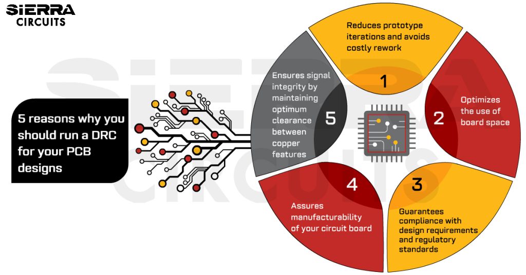
5 reasons why you should run a design rule check for your PCB designs
By running a DRC, you can instantly check if your design adheres to the required standards. You can proactively address the layout issues and ensure manufacturability.
The infographic below highlights five key benefits of performing a DRC.

1. Reduces prototype iterations and avoids expensive rework
Addressing design flaws early in the design phase using DRC helps avoid expensive and time-consuming prototype changes. This makes the product development process faster, reducing the time-to-market and overall costs.
2. Optimizes the use of board space
DRC aids in efficient component placement and routing optimization, guaranteeing effective utilization of available board space.
3. Guarantees compliance with design requirements and regulatory standards
Design rule check ensures that your design adheres to specified requirements and regulatory standards such as IPC-6012. It serves as a virtual quality control, notifying of any deviations from the established design guidelines.
4. Assures manufacturability of your circuit board
Running a DRC ensures that your design aligns with the limitations and capabilities of your CM. This enables you to get the design right the first time. It also paves the way for a seamless transition between prototype and manufacturing stages.
5. Ensures signal integrity by maintaining optimum clearance between copper features
DRC helps maintain signal integrity by imposing appropriate spacing between copper features, reducing the risk of signal integrity issues such as EMI and crosstalk.
To learn how to design a cost-efficient PCB without board respins, download the Design for Manufacturing Handbook.

Design for Manufacturing Handbook
11 Chapters - 96 Pages - 90 Minute ReadWhat's Inside:
- Annular rings: avoid drill breakouts
- Vias: optimize your design
- Trace width and space: follow the best practices
- Solder mask and silkscreen: get the must-knows
Download Now
What are the steps to run a DRC in KiCad version 8?
Start by navigating to File and configuring the design rules in the Board Setup dialog. Use the design rule checker to verify the constraints and connectivity against the schematic and netlist.
Setting design rules in KiCad is crucial for controlling the behavior of the interactive router, managing the filling of copper zones, and ensuring the accuracy of the design rule checker. You can modify design rules at any time. However, it is advisable to establish all known design rules at the outset of the board design process.
KiCad’s design rule checker helps you to ensure that the PCB complies with the requirements set in the Board Setup dialog. It also verifies that all pads are connected in accordance with the netlist or schematic.
The infographic below summarizes the steps to set up and run DRC in KiCad version 8:

Configuring design rules in KiCad
Step 1: Go to File.
Step 2: Select Board Setup.
Step 3: Choose Design Rules to access the complete list of design rules.
You can now configure the design rules according to your project requirements.

The design rules dialog provides you with a comprehensive display of standard rules. These rules are categorized based on their specific functionalities. Let’s look at the design rules available in KiCad:
Constraints
The design rules for constraints include minimum clearance required for copper, holes, microvia, silkscreen, arc/circle approximated by segments, zone fill strategy, and length tuning.

Pre-defined sizes
The pre-defined sizes section enables you to define the preferred dimensions for tracks and vias that are readily accessible for use while routing.

Teardrop
Here, you can establish default settings for different kinds of teardrops (circular, rectangular, and track-to-track). To add teardrops for individual vias and pads, double-click the pad or right-click on the pad and select Pad Properties.
You can also quickly add teardrops to existing connections. To do this, go to Edit and click on Edit teardrops.

Length-tuning patterns
In this section, you can establish default settings for various length-tuning patterns, such as single-track length, differential pair length, and the skew between differential pairs.

Net classes
The net classes rules section enables you to set up specific routing and clearance regulations for different classes of nets. Every class can be assigned specific values for copper clearance, track width, microvia, via, and differential pair sizes.

Custom rules
The custom rules section contains a text editor for creating design rules using the custom rules language. These rules are meant to address requirements that aren’t covered by the fundamental constraints or net class settings.

Violation severity
The violation severity section allows you to change the level of seriousness associated with each sort of design rule evaluation. You can specify whether a rule should result in an error marker, a warning marker, or be ignored.

To learn how to create component libraries and high-speed schematics in KiCad, download our e-book.
KiCad Design Guide
10 Chapters - 161 Pages - 180 Minute ReadWhat's Inside:
- Creating a component symbol library
- Setting up board parameters and rules
- How to route differential pairs
- How to place of components
Download Now
Generating a design rule check report in KiCad
Step 1: Navigate to the Inspect.
Step 2: Choose Design Rules Checker and click on DRC.

If your design has any discrepancies, it will be displayed as shown above.
The top section of the DRC Control window comprises a set of options that are responsible for regulating the behavior of the design rule checker:
Refill all zones before performing DRC: When this feature is enabled, zones will be automatically refilled each time the design rule checker is initiated. Disabling this option could lead to inaccurate DRC outcomes if zones haven’t been manually refilled.
Report all errors for each track: This option reports all clearance errors per track segment, while disabling it only reports the first error. This option may slow down the design rule checker.
Test for parity between PCB and schematic: When enabled, the design rule checker checks both PCB design rules and discrepancies between the schematic and PCB.
Check out Sierra Circuits’ KiCad Quote Plugin to get an instant quote for your PCB design without exiting the KiCad UI.
How to run a design rule check in Altium Designer
Configure the design rules first using Altium Designer’s PCB Editor. These rules define the requirements that the PCB layout must follow. Then navigate to the Tools menu and select Design Rule Checker.
Here’s an infographic that summarizes the steps to run a DRC in Altium Designer.

Configuring design rules in Altium Designer
Follow these steps:
Step 1: Navigate to the Design menu.
Step 2: Select the Rules option.
Step 3: Click on Rules, and then the PCB Rules and Constraints Editor window opens.
Here, you can create and modify rules related to different design aspects, such as clearance, routing, and impedance.

Let’s look at the design rule categories and their DRC parameters in Altium Designer:
| Design rule category | DRC parameters |
|---|---|
| Electrical | Clearance, short-circuit, un-routed net, unconnected pin, and modified polygon. |
| Routing | Width, routing topology, routing priority, routing layers, routing corners, routing via style, fanout control, and differential pairs routing. |
| SMT | SMD to corner, SMD to plane, SMD neck-down, and SMD entry. |
| Mask | Solder mask expansion and paste mask expansion. |
| Plane | Power plane connect style, power plane clearance, and polygon connect style. |
| Testpoint | Fabrication testpoint style, fabrication testpoint usage, assembly testpoint style, and assembly testpoint usage. |
| Manufacturing | Minimum annular ring, acute angle, hole size, layer pairs, hole-to-hole clearance, minimum solder mask sliver, silk-to-solder mask clearance, silk-to-silk clearance, net antennae, and board outline clearance. |
| High speed | Parallel segment, length, matched lengths, daisy chain stub length, vias under SMD, maximum via count, and maximum via stub length (back drilling). |
| Placement | Room definition, component clearance, component orientations, permitted layers, nets to ignore, and height. |
| Signal integrity | Signal stimulus, overshoot – falling edge, overshoot – rising edge, undershoot – falling edge, undershoot – rising edge, impedance, signal top value, signal base value, flight time – rising edge, flight time – falling edge, slope – rising edge, slope – falling edge, and supply nets. |
Once the design rules have been established, follow these steps to run a design rule check:
Step 1: Navigate to the Tools menu.
Step 2: Select Design Rule Checker.
Step 3: In the Design Rule Checker window, click on Run Design Rule Check to run the test.

The design rule checker window is broadly categorized into two main areas:
- Online design rule check
- Batch design rule check
The online design rule-checking process operates in the background, providing real-time monitoring and detection of design rule violations. It promptly identifies and flags any violations. While routing, it can even automatically prevent such errors from occurring.
Meanwhile, the batch DRC feature enables you to initiate a manual verification at any point. To enable this feature, you need to check the respective box in the Design Rule Checker dialog, as shown below.


Generating a DRC report in Altium Designer
Step 1: Click on the Report Options tab within the Design Rule Checker dialog.
Step 2: Check Create Report File and then click on Run Design Rule Check.

The report provides a comprehensive list of rules that were subjected to testing during the batch-checking process in accordance with the specifications outlined in the Design Rule Checker dialog.
Need help ensuring your PCB design passes DRC checks for manufacturing? Our engineering team can assist you with design rule validation, DFM analysis, Gerber/ODB++ file review, and manufacturing constraint checks to avoid costly respins.
You can book a meeting with our experts or call us at +1 (800) 763-7503.

How to run a DRC in Cadence® Allegro® PCB designer
After defining the required constraints (design rules), navigate to Display and Update DRC to start the design rule check.
The infographic below shows the steps to run DRC in Cadence Allegro PCB Designer.

Configuring design rules in Cadence Allegro PCB Designer
Follow these steps to set up your design rules in Cadence Allegro PCB Designer:
Step 1: Navigate to the Setup menu and select Constraints
Step 2: Choose Modes to open the Analysis Modes dialog. Here, you can enable/disable constraints according to your project requirements.

The analysis modes settings window provides you with a comprehensive display of standard rules that are categorized based on their specific functionalities. This allows you to enable all the rules according to your project requirements.
Let’s look at the standard design rule categories available in the analysis mode:
| Design rule category | DRC parameters |
|---|---|
| Electrical | Stub length/net schedule, max via count, match via count, max exposed length, propagation delay, relative propagation delay, max parallel, impedance, total etch length, all differential pair checks, and layer sets. |
| Physical | Min neck width, max line width, allow etch on subclass, allow T junctions on subclass, min blind/buried via stagger, max blind/buried via stagger, pad-pad direct connect, and vialist DRC. |
| Spacing | Enable/disable different spacing constraints between attributes such as line, thru pin, SMD pin, test pin, thru via, test via, bond finger, hole, and min BB via gap. |
| Same net spacing | Covers all relevant spacing checks between attributes such as line, thru pin, SMD pin, test pin, thru via, test via, bond finger, hole, and min BB via gap. |
| Assembly | Wire to wire, wire to wire end, wire to pin, wire to bond finger, minimum bonding wire length, maximum bonding wire length, wire to die edge angle, bond wire diameter, and bond finger to component. |
| Design for fabrication | Outline, mask, annular ring, copper features, copper spacing, and silkscreen. |
| Design for assembly | Outline, package-to-package spacing, spacing, and paste mask. |
| Design for test | Outline, mask, and silkscreen, spacing, and probe. |
Next, you need to set different constraint values for electrical, physical, and spacing constraints. Here, you can set allowable maximum and minimum values for different elements.
Spacing constraint
Spacing constraints refer to the rules that dictate the maximum and minimum spacing required between elements on different nets. It is the distance that should be maintained between various components or traces on the circuit board. Spacing constraints help prevent issues such as short circuits, crosstalk, and EMI.
 Setting up spacing constraints in Cadence Allegro PCB Designer
Physical constraint
It establishes rules that govern the creation of interconnections of an individual net.
They define specific limitations to ensure:
- Consistent line widths across different areas and layers
- Permissible connections on a specific layer
- Acceptable vias for use with a specific net
 Setting up physical constraints in Cadence Allegro PCB Designer
Electrical constraints
Electrical constraint sets consist of rules that govern the electrical behavior of components such as nets, buses, and differential pairs. They provide guidelines on how signals should propagate through different paths, ensuring that they arrive at their intended destinations without propagation delay.

Generating DRC report in Cadence Allegro PCB Designer
Follow these steps to generate DRC in Cadence Allegro PCB Designer
To DRC check in Cadence Allegro PCB Designer:
Step 1: Navigate to the main menu.
Step 2: Select Display and then Status
Step 3: Click on update DRC to run standard design rule checks.

Step 4: Navigate to the Export menu in Cadence Allegro PCB Designer.
Step 5: Select Quick Report and choose Design Rule Check to view the DRC report.

The resulting Design Rule Check (DRC) report conveniently appears in a new tab, facilitating easy access and review. Also, see design rule check vs. design for manufacturing.
Key takeaways
- To run a DRC, you need to first configure the design rules in your EDA.
- Altium Designer, Cadence Allegro PCB Designer, and KiCad offer tools for configuring and managing design rules, allowing for efficient categorization and customization based on project requirements.
Knowing how to effectively navigate and utilize DRC procedures in EDA tools helps you to identify and rectify potential design flaws early in the design phase. This reduces prototype iterations and ensures a quick transition to the PCB manufacturing stage.
Need assistance in designing your circuit board? Post your questions in the SierraConnect forum. We will be pleased to assist you!

About Mohamed Faheemuddin : Mohamed Faheemuddin is a mechanical engineer. His passion for electronics drew him to the PCB industry. With an experience of over 3 years in the PCB industry, he specializes in developing articles for engineers and hardware designers.


