


Contents

On-demand webinar
How Good is My Shield? An Introduction to Transfer Impedance and Shielding Effectiveness
by Karen Burnham
Drilling is the process of creating holes in a circuit board for component mounting and layer-to-layer electrical connections.
This process must be carefully implemented as poor drilling can lead to breakout, resin smear, and rough hole walls in high-density PCB designs.
As a PCB designer, understanding drilling limitations, aspect ratio requirements, and drill-to-copper clearance helps reduce board failures and optimize production yield.
In this article, you’ll learn about mechanical and laser drilling, PCB drilling processes, drill-related defects, and DFM guidelines.
Highlights:
- Maintain adequate drill-to-copper clearance to improve via reliability and copper plating quality.
- Mechanical drilling supports standard PCB fabrication, while laser drilling enables precise microvias for high-density designs.
- Poor drilling accuracy can lead to breakout, resin smear, burr formation, barrel cracks, and conductivity failures.
- Check drill sizes, annular ring requirements, and plated/non-plated hole definitions during PCB DFM checks.
What are the different PCB drilling methods?
There are two types of drilling techniques: mechanical and laser drilling.

1. Mechanical drilling
It uses rotating drill bits to create holes in printed circuit boards. The smallest hole diameter that can be drilled by these drills is about 6 mil (0.006”).
Mechanical drill limitations
When used on softer materials like FR4, the mechanical drills can deliver 800 hits. For denser materials like Rogers, the lifespan is reduced to 200 counts.
If a PCB manufacturer ignores this, faulty holes will result, turning the board into scrap. The superior Hitachi drilling machines are implemented at Sierra circuits with a 1 mil hole placement tolerance.
2. Laser drilling
It is a non-contact process in which the workpiece and the tool do not come in contact. A laser beam is used to remove board material and create precise holes. Here, the drill depth can be effortlessly controlled.
The laser technology is used to drill controlled-depth vias with ease. Here, a minimum hole diameter of 2 mils (0.002”) can be drilled with precision.
Laser drilling limitations
A circuit board is made of copper, glass fiber, and resin. These PCB materials have different optical properties, making it difficult for the laser beam to burn through a board efficiently.
The cost of the process is also comparatively high in the case of laser drilling.

PCB Design for Assembly Handbook
6 Chapters - 50 Pages - 70 Minute ReadWhat's Inside:
- Recommended layout for components
- Common PCB assembly defects
- Factors that impact the cost of the PCB assembly, including:
- Component packages
- Board assembly volumes
Download Now
It is better if the designer understands what happens on the shop floor to get a better perception of how the design is brought to life.
With this insight, the board designer ensures that the designs are manufacturable. This, in turn, reduces the cost, and the product can be delivered in a minimum turnaround time.
How is PCB drilling performed?

The drilling process begins after lamination. The laminated boards are loaded on a panel of exit material on the drill bed. The exit material lessens the burr formation. Burr is the protruding part of copper formed when the drill spindle penetrates through the board.
On top of this panel, more stack-ups are loaded and are carefully aligned. In the end, a sheet of aluminum foil is placed over this entire stack-up. The Aluminium foil avoids entry burr and also dissipates the heat generated by the rapidly spinning drill bit.
Once the required number of holes is drilled, the boards are sent for the deburring and desmearing process.
Tool geometries must be considered since the quality of the drilled hole is crucial. High-speed steel (HSS) and tungsten carbide (WC) are commonly used drill bit materials for drilling composites.
Carbide tools offer better tool life during the machining of glass fiber-reinforced polymer (GFRP). The cemented carbide drills are generally used in PCB drilling.
What are the point and helix angles in circuit board drill bits?

The point angle is located at the tip of the drill bit and is measured between its primary cutting edges. The helix angle is the angle formed between the flanks of a drill bit at their intersection points.
Drill tips typically have a point angle of 130° and a helix angle between 30° and 35°.

What is a CNC drill machine? How does it work?

A computer numerically controlled (CNC) drilling machine is a preprogrammed device used to create holes in printed boards. It drills according to the predefined XY coordinates fed into the CNC system.
The spindles rotate at a high RPM to ensure an accurate drill hole is found on the board. When the spindle rotates rapidly, heat is generated due to the friction between the hole wall and the spindle.
This melts the resin content on the hole walls, resulting in a smear of resin. Once the required holes are drilled, the exit and entry panels are discarded. This is a small gist of what happens on the shop floor.
Unlike the etching and plating process, drilling doesn’t have a fixed duration. The drilling time varies on the shop floor depending on the number of holes drilled.
This is what happens behind the curtains in the circuit board manufacturing unit. To know more about computer-aided manufacturing related to PCB, read What is CAM or computer-aided manufacturing?
Two significant aspects to be considered in the drilling process:
- The aspect ratio
- Drill to copper clearance (Drill to the nearest copper feature)
Aspect ratio
Aspect ratio is the ability to effectively plate copper inside the holes(vias). Copper plating of the interior part of holes is a tedious task when the diameter is decreased and the depth is increased.
This requires a plating bath with a high throwing power so that the liquid can gush into the tiny holes.
Aspect ratio (AR) = (Depth of the hole/ Diameter of the drilled hole)
The aspect ratio is 10:1 for through holes and 0.75:1 for microvias.
Typically, for a 62-mil PCB, the minimum drill size is 6 mil.
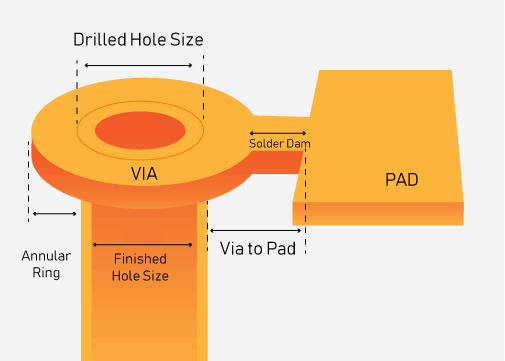
Drill to copper

The drill-to-copper is the land clearance between the edge of a drilled hole and the nearest copper feature. The nearest copper feature can be a copper trace or any other active copper region.
This is the deciding factor since even a small deviation will lead to circuit disruption. The typical drill-to-copper value is around 8 mils.
Minimum clearance = annular ring width + solder mask dam clearance
Classification of holes
PCB drilled holes are categorized into plated through-holes (PTHs) and non-plated through-holes (NPTHs) based on their function in the circuit board.
| Feature | PTH | NPTH |
|---|---|---|
| Conductivity | Conductive | Non-conductive |
| Primary purpose | Establishes electrical interconnections between PCB layers | Provides mechanical support and mounting holes for components and hardware |
| Signal transmission | Carries signals and power between layers | Does not carry signals or power |
| Typical applications | Vias, through-hole component leads, and layer-to-layer connections | Component mounting holes, tooling holes, and mechanical fastening points |
Design considerations for PTHs and NPTHs
Drilling holes in a circuit board is not as easy as it sounds. This requires great precision and should adhere to certain design rules. Let us have a look at these requirements for NPTH and PTH.
Non-plated through-hole (NPTH)
- Finished hole size (minimum)= 0.006″
- Edge-to-edge clearance (from any other surface element) (minimum)= 0.005″
Plated through-hole (PTH)
- Finished hole size (Minimum) = 0.006″
- Annular ring size (Minimum)= 0.004”
- Edge-to-edge clearance (from any other surface element)(minimum) = 0.009″
6 common PCB drilling defects
After repeated usage, drilling tools tend to wear and break. This leads to the following problems:
1. Inaccurate hole location
The accuracy is compromised when the drill bit fails to hit the preferred spot and shifts away on the same axis. The shifts in the drilled hole will give rise to tangency or breakout in annular rings.
2. Roughness inside the drilled hole
Roughness leads to a non-uniform plating of copper. This results in blowholes and barrel cracks. It can also result in lower insulation resistance due to the penetration of copper plating solution into the hole wall.
3. Resin smear
The resin in the board melts due to the heat generated during the drilling. The resin sticks to the hole walls and is called a resin smear. This again results in poor copper plating and leads to conductivity failure between the via and the interior layers of the circuit. The resin smear is removed by a chemical solution.
4. Entry and exit burrs
Burr is the unwanted part of copper sticking out of the hole after the drilling process. They are mostly seen on both the top surface and the bottom surface of the printed circuit board stack-up.
5. Nailhead
If the nailheads are improper, then there is a chance of copper bends in the inner layers while drilling. These copper bends cause uneven plating and result in conductivity issues.
6. Delamination
The partial separation of the circuit board layers is considered delamination. Improper drilling causes delamination.
All these irregularities ruin the board’s integrity, which has been a nightmare for the manufacturers. For these reasons, our in-house design engineers whimsically define PCB as “problems come back!”
In order to eliminate these flaws, scholars have researched the drilling process and design structure and have come up with the following solutions:
Remedies:
- Desmear process: It is a chemical process where the melted resin deposited on the hole walls is removed. This process eliminates unwanted resin and enhances electrical conductivity through the vias.
- Deburr process: It is a motorized process that eradicates the elevated ends (crowns) of the metal (copper) called burrs. Any debris left out within the holes is removed through the deburring process. The desmearing process is repeated after deburring.
- Laser drilling: Delamination can be avoided by using laser drills. As mentioned earlier, in laser drilling, the workpiece and the tool do not come into contact, thus eliminating delamination.
Need help optimizing your PCB drill design? Our engineering team can help you select the right drill sizes, verify aspect ratio requirements, and review drill-to-copper clearances.
You can book a meeting with our experts or call us at +1 (800) 763-7503.

Take a look at the quick DFM guidelines below, which can help you save a few bucks.
PCB designers’ DFM checklist for reliable drilling
PCB designers should validate drill sizes, aspect ratio requirements, hole definitions, and drill tolerances.
Here’s a detailed checklist:
- The aspect ratio must be kept to a minimum to avoid drill wear.
- An increase in different drill sizes in the design ( having different hole sizes) will call for increased drill bits (drill bits will be changed for specific sizes). If you restrict the implementation of different drill sizes, it will cut down the drill time.
- Check:
- If non-plated drills have connections.
- For drill count/size between the drill file and the fab print.
- If drill type is defined (PTH / NPTH).
- For close holes less than 0.006″, if yes, it must be addressed.
- For mouse bites.
- If the drills and other features on the copper layers are falling outside the board profile.
- If via sizes should be dropped to meet the minimum aspect ratio (A/R) requirement, looking at drill tolerance.
- For plated drill tolerance less than +/- 0.002″ and for NPTH, drill tolerance of +/- 0.001.
- Fab drawing for arcs showing NPTH drill/slot or cutout locations that are missing in the drill file.
- For the via filling requirement with respect to assembly guidelines.
Sierra Circuits fabricates high-reliability PCBs using precision mechanical drilling and advanced hole quality control processes to support complex and high-density designs. To learn more, see our rigid PCB manufacturing capabilities.
The drilling process has been optimized in recent years compared to earlier technologies. With the exponential growth in the circuit board industry, drill precision is reaching close to perfection.
Do you want to know more about back drilling? Read PCB back drilling to learn improve signal integrity in high-speed designs.
We believe now you have a better picture of how the PCB drilling process is done. It looks quite complicated, doesn’t it? Don’t worry! Just submit your design files (Gerber) to Sierra Circuits. Allow us to drill while you sit back and relax.

About Rahul Shashikanth : Rahul Shashikanth is an electronics and communication engineer with over 8 years of experience in publishing technical articles on PCB design, manufacturing, and assembly. He is currently the content marketing manager at Sierra Circuits.


Start the discussion at sierraconnect.protoexpress.com