


Contents

On-demand webinar
How Good is My Shield? An Introduction to Transfer Impedance and Shielding Effectiveness
by Karen Burnham
PCB layout design tools assist you with schematic creation, layout design, trace routing, BOM validation, and design file generation. The factors that determine a good EDA tool are its user interface, 3-D visualization, and routing and simulation capabilities.
Being a board designer, you need to know the functionalities of some of the best design tools before you choose the right one.
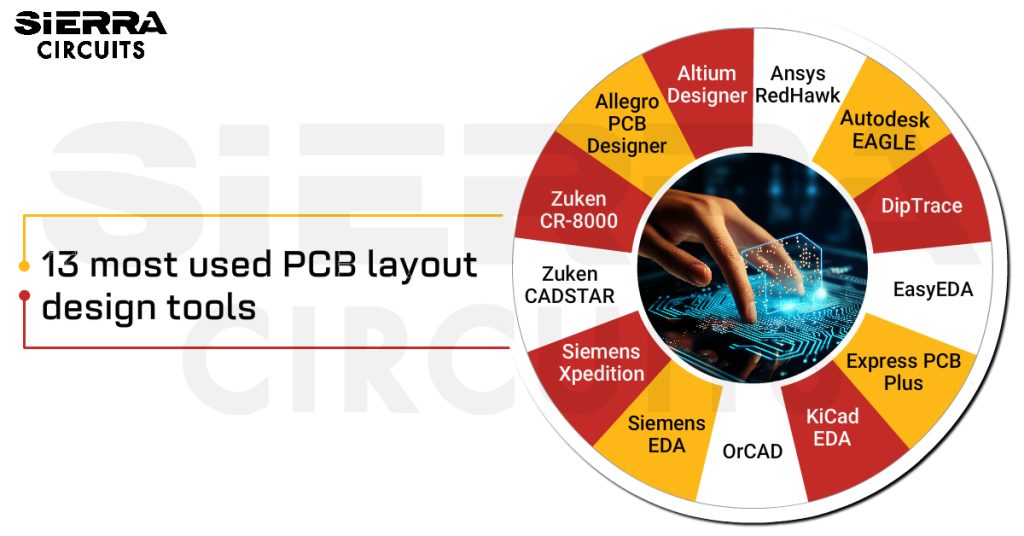
Here’s the list of 13 most used EDA tools (in alphabetical order).
- Allegro PCB Designer
- Altium Designer
- Ansys RedHawk
- Autodesk EAGLE
- DipTrace
- EasyEDA
- ExpressPCB Plus
- KiCad EDA
- OrCAD
- Siemens EDA (Mentor Graphics PADS)
- Siemens Xpedition
- Zuken CADSTAR
- Zuken CR-8000
What’s an EDA tool?

EDA tools or PCB layout tools automate circuit board design processes such as schematic creation, layout design, trace routing, and component footprint creation. The software also enables you to simulate your design and verify the functionality of your application.
Allegro PCB Designer
This tool is designed by Cadence Design Systems. If you require a strong and dependable layout design tool, this is an excellent option.
Signal integrity analysis
Allegro PCB Designer is integrated with a simulator, which helps you conduct signal integrity analysis of your board during the design phase. It helps you identify design issues that may lead to noise, crosstalk, and timing errors.
Advanced routing options
Allegro offers several advanced routing features that help you build complex PCB designs. You can define various routing constraints, such as length matching for differential pairs, controlled impedance, and crosstalk prevention.
These features become essential if you generally work on high-speed designs. Allegro has a steep learning curve, which can be challenging for you initially, but with time you will be acquainted with the tool.
Pre-built electronic component library
The tool comes with a large component library that provides a wide range of pre-built electronic components. This feature offers ready-to-use components and speeds up the component placement process in your layout.

Dilip Kumar, Senior PCB Design Manager, says “Most designers prefer Altium and Allegro due to their accurate constraint setting features. This makes it easy to realize all the DFM and DRC requirements.”

High-Speed PCB Design Guide
8 Chapters - 115 Pages - 150 Minute ReadWhat's Inside:
- Explanations of signal integrity issues
- Understanding transmission lines and controlled impedance
- Selection process of high-speed PCB materials
- High-speed layout guidelines
Download Now
Altium Designer
Altium Designer is a comprehensive software tool preferred by most designers. You can use it for designing advanced boards such as HDI, flex and rigid-flex PCBs. Here are a few unique features of this designer tool.
Easy-to-use and intuitive interface
The software is user-friendly and suitable for both novice and experienced users. The UI has organized menus, toolbars, and panels to ensure a seamless and effective design workflow.

3D visualization

A robust 3D visualization feature lets you see your board in three dimensions during the design phase. This feature helps you in verifying component orientation and other physical constraints of your board.
Collaborate with other designers
Altium Designer offers you a collaborative setting where you can network with several designers at once. This facilitates teamwork and speeds up the design process. This option helps when creating a board layout through a modular design approach.
Altium Designer is a premium software, and its license costs more than other circuit design tools. Consumers or small businesses on a tight budget may find this an expensive tool.
If you are looking for the most reliable circuit design software in the market, Altium Designer remains an ideal choice for many professional designers and engineers. This is due to its diverse features, extensive integration capabilities, and user-friendly interface.
Allan Knox, Senior PCB Design Engineer at Sierra Circuits, explained, “Altium and Allegro PCB layout tools have more advanced features and a larger user base, where you can click on any entity and access information. Beginners can consider Eagle and KiCad as they are open-source EDAs”

Ansys RedHawk
Ansys RedHawk provides a complete software solution to design a PCB and test for its power integrity, signal integrity, and thermal stability.
Power integrity analysis
RedHawk has a strong power integrity analyzer that lets you find and fix power distribution errors during the stage. It eliminates the risk of performance degradation caused by voltage fluctuations.
Filters out noise and distortion-related issues
The tool offers advanced signal integrity analyses to rectify delay, crosstalk, noise, and PCB jitter. This will help you maximize signal integrity and reduce noise-related problems.
IC electro-thermal simulator
RedHawk’s IC electro-thermal simulator can improve temperature distribution within ICs and systems on chips. This improves chip dependability, prevents overheating, and identifies possible hotspots.
Autodesk EAGLE
Autodesk EAGLE offers a straightforward user interface for design operations. Unique features of this EDA tool are discussed below.
Large component library
Eagle provides a large component library with electronic components, symbols, and footprints. This comprehensive collection reduces the time and effort required to create components manually.
To understand the importance of the component library, read the importance of quality PCB libraries.
Integrated with other design products
Eagle connects smoothly with other design software like Autodesk Fusion 360 and Autodesk Eagle Premium. This integration will help you utilize the features that are not present in Autodesk Eagle. As a result, you can speed up the design process and increase work efficiency.
User-friendly and open-ended
Autodesk Eagle is an all-inclusive, user-friendly EDA program that provides a wide range of features. However, if you opt for a free version, functionality will be limited.
This tool is a good option for small firms and designers looking for reasonably priced PCB design software.
DipTrace
Hierarchical schematic capture
DipTrace PCB layout tool comes with a multi-sheet schematic capture capability. This feature enables you to create independent subcircuits within the main schematic. These subcircuits can have their own submodules and can be further divided, making it easier to navigate among different circuit modules.
Wide range of component library
The tool has more than 160000 components and thousands of land patterns designed as per the IPC-7351 standard. It also allows you to design new components using custom templates. Features such as bulk pin naming, pad renumbering, and bus management tools can speed up the design process.
EasyEDA
EasyEDA is an open-source web-based EDA. It offers a collaborative platform that includes schematic capture, layout design, component library, and project management.
Access to real-time component inventory
The tool is integrated with real-time component inventory, using which you can quickly view the price, datasheets, and stocks of the parts. This speeds up the component selection process.
ExpressPCB Plus
Powerful auto-router
Auto-routing is one of the primary features of this tool. It saves a lot of time by automatically determining suitable routing patterns. The software uses cutting-edge algorithms to shorten traces, reduce interference, and improve signal integrity.
Diverse component library
The tool comes with an extensive component library that supports parts from multiple suppliers. You can easily locate and include components in your designs from this library.
ExpressPCB Plus also features 3D visualization and DRC, which is essential for building an error-free circuit board.
Kicad EDA
Aspiring PCB designers and small enterprises seeking handy EDA software could consider KiCAD. Features of this EDA include:
Open source EDA
It is an open-source and free application. This makes it a great option for students or beginners who are looking for a robust design tool.
Active and supportive community
KiCad’s user and developer communities are active and thriving. This community actively participates in software development and design data exchange.
Cross-platform compatible
KiCad is available for various operating systems, such as Linux, Windows, and macOS. With its cross-platform adaptability, you can quickly share design information with a co-designer who is working on a different operating system.
Download our KiCad quote plugin to get an instant quote for your design without leaving the KiCad UI.
KiCad Design Guide
10 Chapters - 161 Pages - 180 Minute ReadWhat's Inside:
- Creating a component symbol library
- Setting up board parameters and rules
- How to route differential pairs
- How to place of components
Download Now
Design rule check (DRC)
The DRC function verifies design data against predefined rules. Using this, you can spot errors such as overlapping components, clearance violations, and incorrect trace widths.

Although KiCad’s interface has evolved over time, it is still less intuitive when compared to other commercial solutions. If you are used to other PCB design tools, you may take time to adjust to the user interface.

OrCAD
OrCAD offers an intuitive interface and advanced simulation capabilities, empowering designers to create and test electronic circuits efficiently. Check out the following features of OrCAD:
Advanced mixed-signal simulation
ORCAD provides advanced simulation capabilities, including analog, digital, and mixed-signal simulations. This feature is essential for analyzing a system’s interaction between analog and digital components. Mixed-signal simulation helps identify potential issues such as noise coupling, signal integrity problems, and voltage spikes.
User-friendly interface
ORCAD is known for its easy-to-use interface for both beginners and experienced users. It is integrated with the Cadence simulation software Sigrity. Sigrity analyzes power distribution networks within electronic designs. It can simulate power delivery, voltage drop, and noise propagation throughout the PDN. Also, engineers can simulate high-speed signal behavior, including signal attenuation, skew, and eye diagram analysis, using this software.
Extensive component libraries
The latest version of OrCAD comes with extensive component libraries covering a wide range of electronic components. This helps designers save time during the design process.
Siemens EDA (Mentor Graphics PADS)
Mentor Graphics PADS, commonly known as PADS, was recently taken over by Siemens. The unique features of this PCB layout tool are:
3D component placement
This feature lets you position components in three dimensions during the design phase. You can also optimize component locations and orientations to ensure reliable electrical connectivity by considering thermal and mechanical attributes.
Automated manufacturing file generation
The generation of design files, such as Gerber and ODB++, can be automated. This ensures that you have all the essential manufacturing files required by your fabricator.
Siemens Xpedition
Siemens Xpedition provides an integrated design flow. It optimizes PCB designs with industry standards and enhances team collaboration. Learn the distinct features of this PCB layout tool here:
Interactive routing
Xpedition offers various routing modes within the interactive routing feature, including single-track, differential pair, and multi-track routing. Engineers can switch between these modes based on the design requirements. Also, it provides automatic routing assistance features within the interactive routing.
Integrated design flow
Xpedition offers a highly integrated design flow, combining schematic capture, PCB layout, and simulation into a single environment. It includes advanced DRC capabilities to verify circuit designs against industry standards and best practices. Xpedition offers a fully parallel, collaborative design environment where multiple teams can work on the same design in real time.
Comprehensive signal and power integrity analysis
It incorporates comprehensive design analysis capabilities, including thermal, signal, and power integrity analysis. The layout tool enables designers to model decoupling capacitors and analyze PDN resonance. This ensures an adequate power supply with stable voltage levels.
Need help in designing reliable PCBs? Our engineering team can help you with thermal management, stack-up design, and DFM analysis.
You can book a meeting with our experts or call us at +1 (800) 763-7503.

Zuken CADSTAR
The tool supports multiple industry-standard formats and libraries, which will help you collaborate with other design tools more easily. Other features of this EDA include:
Excellent schematic capture
CADSTAR schematic capture provides a quick and efficient way to capture your schematic, design intent, and rules into the PCB layout. In addition to this, the component library has access to more than 250000 parts.
Optimized routing for high-speed designs
Zuken’s Place and Route Editor is optimized to meet all your DFM and signal integrity requirements. It also provides additional functionality specific to high-speed applications such as DDR-2, DDR-4, DDR-5, and PCIe.
Design migration
Designs created using Zuken CADSTAR can be easily imported to other PCB design tools such as Siemens EDA, Allegro, and Altium Designer.’
Electrical rule check (ERC)
ERC in DipTrace helps you verify the electrical integrity of your circuit. It checks for common electrical violations such as open circuits, unconnected pins, short circuits, incorrect component orientation, and other design rule violations. By running an ERC, you can prevent potential manufacturing errors and signal integrity issues.
Zuken CR-8000
Zuken CR-8000 stands out for its robust design features and advanced capabilities. The unique features of CR-8000 are:
3D PCB design model
It offers advanced 3D PCB design analysis. With the 3D model, designers can check for the component’s physical layout, trace spacing, trace width, and component/connector clearances. This can help resolve DFM issues early in the design phase.
Concurrent design environment
CR-8000 provides a concurrent design environment where multiple team members work on different design aspects simultaneously.
High-speed circuit design features
This PCB layout tool is tailored explicitly for high-speed designs. It includes signal integrity analysis with automated time domain reflectometry, PCB eye diagrams, and EMC simulation. CR-8000 enables designers to simulate the transmission line behavior, considering impedance matching, propagation delay, and signal attenuation.
Understand how AI is improving PCB design efficiency in How AI is transforming the circuit board industry.
PCB layout tools help you in various design aspects, such as schematic capture, component creation, routing, and design rule verification. Choosing the right EDA tool is crucial to achieving design efficiency. You must consider your expertise, budget, and design requirements before selecting the CAD software.
Let us know your favorite EDA tool in the comments section.

About Poulomi Ghosh : Poulomi is a microwave engineer specializing in EMI, EMC, RF, and high-speed electronics. As a senior technical writer at Sierra Circuits, she creates advanced engineering articles and webinars for hardware engineers and PCB designers.


