


Contents
In this article, we will discuss the role of copper wrap plating in increasing the reliability of via structures.
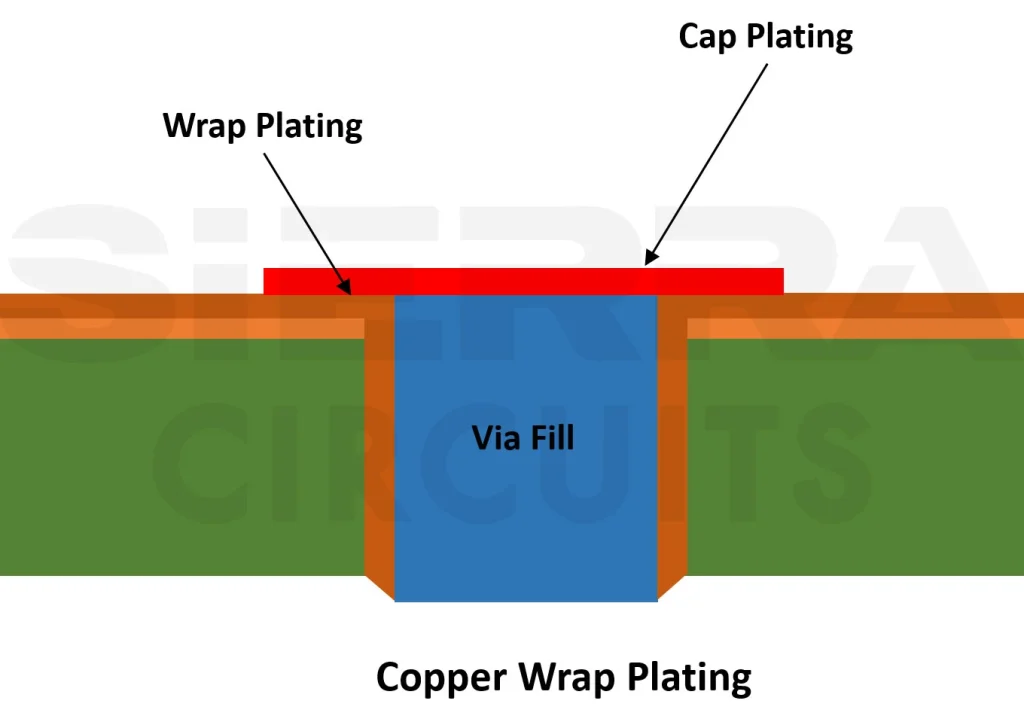
What is copper wrap plating?
Electrolytic hole plating extending to the surface from a plated via structure is known as the copper wrap. (From IPC-T-50 standards). In simple words, wrap plating is the extended copper plating from the via hole that wraps around the surface foil.

Why is copper wrap plating required?
Wrap plating is used to increase the reliability of via-in-pads and was introduced in the IPC standard IPC-6012B Amendment 1.
Copper wrap plating structures
The IPC 6021B standard includes a copper wrap plating requirement for via-in-pad structures. The filled copper plating should continue around the edge of the via hole and extend onto the annular ring surrounding the via pad.
The requirement enhances the reliability of the via plating and can potentially minimize failure due to cracks or separation between the surface features and the plated via-hole.
Filled copper wrap structures are of two types. In one method, a continuous copper film can be applied to the interior of a via, which can then wrap over the top and bottom layers at the via ends.
This plating will then form the via pad and trace, which leads to the via, generating a continuous copper structure.
In another approach, the via can have a separate pad formed around the via ends. This separate pad layer is meant to connect to ground planes or traces.
The next step would be the copper wrap plating which fills the via and wraps over the top of the external pad, creating a butt joint between the via pad and the copper fill plating.
Even though there is a certain extent of bonding between the via pad and the fill plating, the two plating structures do not fuse completely together and form a single continuous structure.

Design for Manufacturing Handbook
11 Chapters - 96 Pages - 90 Minute ReadWhat's Inside:
- Annular rings: avoid drill breakouts
- Vias: optimize your design
- Trace width and space: follow the best practices
- Solder mask and silkscreen: get the must-knows
Download Now
What are plated through holes in PCBs?
Through holes in PCB mean the holes that go through all the layers of the PCB. Such holes can either be plated through holes (PTH) or non-plated (NPTH).
While plated-through holes have a thin copper layer coating the hole walls, NPTH doesn’t have such a layer. The copper layer in PTH serves the purpose of conduction and providing mechanical stability to the hole.
Also read, what is conformal coating?
What is via-in-pad?
A via in pad is a surface mount pad that serves the dual purpose of a surface mount pad and a via hole. The via can be a through via or blind via and is used to increase component density.

Effect of thermal cycles on copper wrap plating in PCBs
Repeated thermal cycles lead to stress on the plating, via fill materials and laminate interfaces, due to the different CTEs of the material in the interface. This is called an expansion mismatch, and the magnitude of the mismatch is a function of the number of layers, the CTE of the materials, and the temperature.
Reliability under thermal cycling
When a PCB is subjected to thermal cycles, volumetric expansion generates compressive or tensile stress on the copper wrap plating, via fill material, and laminate interfaces.
Stress on the copper wrap plating can cause the plating in the via barrel to crack and get disjointed from the butt joint. It is also possible for continuous copper wrap plating to crack at the end of the via.
If the interior of the via detaches from the butt joint, or if the via cracks at the edge of the plating, an open circuit failure will occur in the via. Upon repeated thermal cycling, the board is bound to flex, leading to more failures.
Vias that end closer to the outermost layer of the board are likely to fracture under thermal cycling since the board will flex to a greater extent in these layers.
Even though copper wrap plating structures have the potential for failure, they are still preferred over vias that don’t use this type of plating. The plating provides increased structural integrity to the plating in the via. It also increases the contact area between the via plating and the annular ring.
You can increase the structural integrity of the via wall further by using button plating over the existing copper wrap plating. Such button plating will also wrap over the top and bottom edges of the via, just as in wrap plating.
After this step, the plating resist will be stripped, and the via will be filled with epoxy. The next step would be to planarize the surface, leaving behind a smooth surface.
These steps are the best way to enhance reliability while still meeting IPC 6021B standards. Such plating can also be implemented for buried vias if the buried vias are applied in separate layer stacks.
Also, read 12 PCB Thermal Management Techniques to Reduce PCB Heating
IPC 6012 wrap plating specification
IPC-6012B standard states that copper wrap plating shall be continuous from the filled plated hole onto the external surface of the plated structure and extend by a minimum of 25 microns (984 micro-inches) where an annular ring is required.
Additionally, any reduction of wrap plating by processing such as sanding, etching, and planarization, etc., resulting in insufficient plating is not allowed. IPC-6012B Table 3-2 gives the requirements for copper wrap thickness.
The continuous minimum wrap requirement for class 3 designs is 0.472 mils for a via, 0.236 mils microvia, and 0.276 mils for a buried via.

IPC Class 3 Design Guide
8 Chapters - 23 Pages - 35 Minute ReadWhat's Inside:
- IPC guidelines for manufacturing defects
- IPC standards for assembly processes
- Common differences between the classes
- IPC documents to set the level of acceptance criteria
Download Now
Applications of copper wrap plating
Copper wrap plating is essential to increase the performance of a PCB, and the applications are as follows:
- Increases the reliability of via structures
- Enhances the life of the PCB by preventing the failure of via structures
- Strengthens via connectivity
- Used in all types of PCBs
PCB designers should be familiar with copper wrap plating as a way to increase the reliability of via structures. This will help in optimizing the PCB manufacturing process and increasing production yields while ensuring that manufactured PCBs have enhanced product life.


