


Contents

On-demand webinar
How Good is My Shield? An Introduction to Transfer Impedance and Shielding Effectiveness
by Karen Burnham
Vias are miniature conductive pathways drilled into the PCB to establish electrical connectivity between the different PCB layers. Basically, a via is a vertical trace in a PCB.
What is a via?
Before we dive deep into a via hole, I will just define in simple terms what a PCB is. PCB is the art of transmission of signals under controlled parameters. A printed circuit board is the groundwork for the interconnection of components. The main purpose is to form an electrical connection between the active and passive components without interrupting or interfering with another signal or a connection. So, the basic idea is to form networks of connections without conflicting with one another. Hence, PCB is the connection of components where the connections don’t overlap each other.
To achieve this criterion, PCBs are made up of multiple layers. But how are these multilayers connected to each other in order to establish electrical continuity? This is when a via pops into the picture.
As mentioned before, vias are tiny conductive tunnels that connect different layers of the PCB and allow signals to flow through them. The precision to which a manufacturer can drill a via that meets the designer’s requirement makes that PCB manufacturer the best in the industry. It’s always a good practice to find out your manufacturer’s capabilities before designing your circuit.
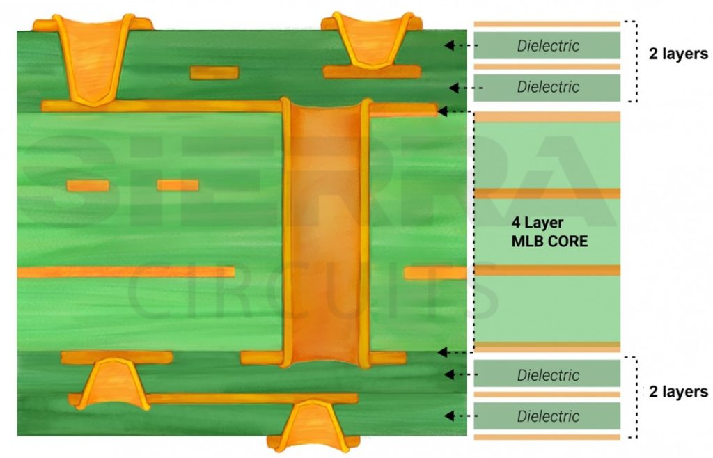
Aspect Ratio for vias in PCBs
Aspect ratio (AR) is the parameter that decides the reliability of a PCB. Let us understand the concept of aspect ratio before discussing more about vias. The aspect ratio is the ratio between the PCB thickness and the diameter of the drilled hole.
Aspect ratio (Through Hole) = (Thickness of the PCB) / (Diameter of the drilled hole)
Since microvias don’t protrude through the entire board, the aspect ratio will be:
Aspect ratio (Microvias) = (Drill Depth) / (Diameter of the drilled hole)
The aspect ratio plays a prominent role in the plating process during PCB manufacturing. The plating solution must flow efficiently inside the drilled holes to achieve the required copper plating. The holes that are small compared with the board thickness can lead to non-uniform or unsatisfactory copper plating. The larger the aspect ratio, the more challenging it is to achieve reliable copper plating inside the vias. Hence, the smaller the aspect ratio, the higher the PCB reliability. At Sierra Circuits, we offer an aspect ratio of 0.75:1 for microvias.


Different kinds of vias in a PCB
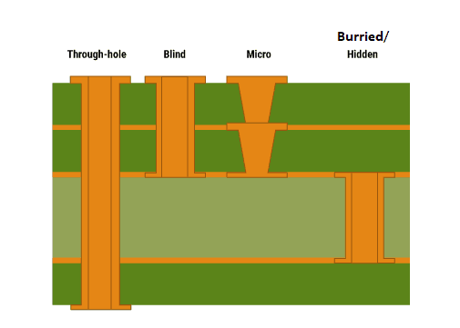
Depending on their functionality, there are different types of vias that are drilled into a PCB.
- Through-hole vias – The hole penetrates from the top to the bottom layer. The connection is established from the top to the bottom layer.
- Blind vias – Hole penetrates from an exterior layer and ends at an interior layer. The hole doesn’t penetrate the entire board but connects the PCB’s exterior layers to at least one interior layer. Either the connection is from the top layer to a layer in the center or from the bottom layer to some layer in the middle. The other end of the hole cannot be seen once the lamination is done. Hence, they are called blind vias.
- Buried vias (hidden vias) –These vias are located in the inner layers and have no paths to the outer layers. They connect the inner layers and stay hidden from sight.
As per IPC standards, buried vias and blind vias must be 6 mils (150 micrometers) in diameter or less.
Microvias
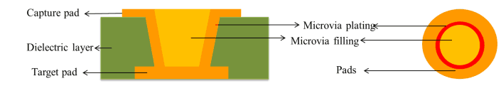
The most commonly known vias are the microvias (µvias). During PCB manufacturing, microvias are drilled by lasers and have a smaller diameter (as small as 4 mils) compared to the standard vias. Microvias are implemented in high-density interconnection or HDI PCBs. The depth of a microvia isn’t usually more than two layers deep since the plating of copper inside these small vias is a tedious task. As discussed earlier, the smaller the diameter of a via, the higher the throwing power of the plating bath should be to achieve electroless copper plating.
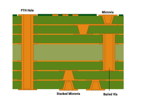
Microvias can be classified into stacked vias and staggered vias based on their location in the PCB layers. Additionally, there is another type of microvias called skipvias. Skipvias skip one layer, meaning they pass through a layer, making no electrical contact with that specific layer. The skipped layer will not form an electric connection with that via. Hence, the name.
Microvias improve electrical characteristics and also allow miniaturization for higher functionality in less space. This, in turn, makes room for large pin-count chips that can be found in smartphones and other mobile devices. Microvias reduce the layer count in printed circuit board designs and enable higher routing density. This eliminates the need for through-hole vias. The microvias’ size and capabilities have successively increased the processing power. Implementation of microvias instead of through-holes can reduce the layer count of PCBs and also ease the BGA breakout. Without microvias, you would still be using a big, fat cordless phone instead of your sleek little smartphone.
Check out our case study on designing 8- and 14-layer HDI PCBs with stacked vias, where our engineers designed blind vias with a 0.75 aspect ratio by optimizing the dielectric thickness and via drill sizes.
Tented Via
Sometimes, a via is covered with a solder mask so that the via isn’t exposed. This is called a tented or covered via.
Since now we have a better understanding of vias, let’s come to the most important part, the via in pad. Sometimes also referred to as via in pad plated over.

High-Speed PCB Design Guide
8 Chapters - 115 Pages - 150 Minute ReadWhat's Inside:
- Explanations of signal integrity issues
- Understanding transmission lines and controlled impedance
- Selection process of high-speed PCB materials
- High-speed layout guidelines
Download Now
Via-in-pad or Via-in-pad Plated Over (VIPPO)
The increasing signal speed, board component density, and PCB thickness have led to the implementation of via-in-pad. The CAD design engineers implement via-in-pad or via-in-pad-plated-over (VIPPO) along with the conventional via structures in order to achieve routability and signal integrity requirements.
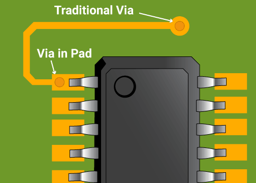
So, what is a via-in-pad? Let me explain. In traditional vias, the signal trace is routed away from the pad and then to the via. You can see this in the above diagram. This is done to avoid seepage of the solder paste into the via during the reflow process. In via in pad, the drilled via is present right below the pad. To be precise, the via is placed within the pad of a surface mount component.
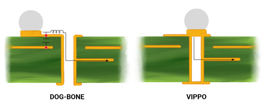
First, the via is filled with non-conductive epoxy, depending on the designer’s requirement. Later, this via is capped and plated to provide conductivity. This technique shrinks the signal path lengths and, as a result, eliminates the parasitic inductance and capacitance effect.
The via-in-pad accommodates smaller component pitch sizes and shrinks the PCB’s overall size. This technology is ideal for BGA footprint components and is an essential part of PCB assembly.
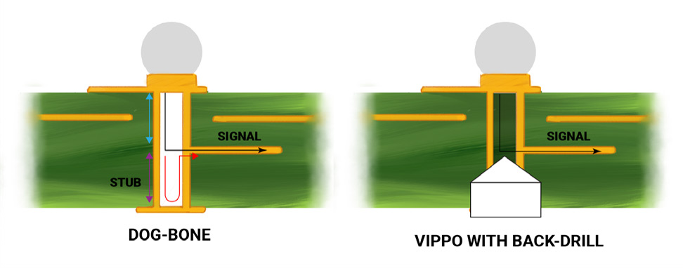
To make things better, the back-drilling process is implemented along with the via-in-pad. The back drilling is performed to eliminate the signal reflections within the unused portion of the via. The unwanted via stub is drilled to remove any kind of signal reflection. This ensures signal integrity.
Quick PCB design tips for vias
Here are a few quick tips that you can consider while employing vias in your design:
- Avoid blind and buried vias unless the design absolutely requires them. These require more drilling time and extra laminations. This can increase the cost of the overall PCB.
- Stacked and staggered vias – Choose staggered instead of stacked vias since the stacked vias need to be filled and planarized. This process is time consuming and expensive as well.
- Keep the aspect ratio minimum. This provides better electrical performance and signal integrity. Also, this results in lower noise, lower crosstalk, and lower EMI/RFI. Read our post on how to avoid crosstalk in HDI substrate.
- Implement smaller vias in high-speed designs since the stray capacitance and inductance are reduced.
- Always select the simplest option that fulfills your design needs. Lowering the complexity of the via leads to decreased turnaround time and manufacturing costs.
- Non-conductive fill is typically adequate for signal routing and is more cost-effective. Therefore, it is better to use non-conductive epoxy wherever possible.
- When you are routing high-speed signals, such as for high-definition multimedia interface (HDMI), it is better to utilize blind or buried vias to eliminate stubs.
- Always use conductive fill for thermal or high-power vias. The higher thermal conductivity will be helpful in heat dissipation required for high-power components.
- When using filled vias, ensure the pad surface after filling is planar, ensuring level component placement to avoid tombstoning defects. A tombstoning defect is where one side of the component detaches from the board during soldering.
- Using vias on differential pair – differential pair routing requires traces to be equal in length to avoid differential time-delay skew. Differential skew is where one signal reaches earlier than the other at the receiver. As far as possible, avoid vias on differential pairs. In case one signal is routed through a via, then the other signal in a differential pair must also be routed through a via. On a differential pair, the number of vias on each trace should be the same.
- Vias on high-speed signals – Vias tend to introduce inductance and capacitance to the circuit. Such characteristics are often negligible in signals that have lower frequencies. When it comes to high-speed signals, vias may significantly affect signal integrity. Therefore, it is better to avoid using vias on high-speed signals.
Try our PCB Via Quiz
In conclusion, vias are basically wells, but not big enough to drop a coin and make a wish. The via technology implemented by your PCB manufacturer could make or break your product. The next time you run into a wishing well, do remember to wish for a perfect wish. Check out our next article in this series on designing vias with current carrying capacity.
For more design information, contact our DESIGN SERVICE team.
About Rahul Shashikanth : Rahul Shashikanth is an electronics and communication engineer with over 8 years of experience in publishing technical articles on PCB design, manufacturing, and assembly. He is currently the content marketing manager at Sierra Circuits.


