


Contents

On-demand webinar
How Good is My Shield? An Introduction to Transfer Impedance and Shielding Effectiveness
by Karen Burnham
Balanced copper distribution in PCBs ensures uniform copper across all layers, improving mechanical stability. Imbalance can lead to defects such as warpage, bow, twist, and resin voids, affecting mechanical stability, signal integrity, and board performance.
As a printed circuit board designer, you should maintain stack symmetry, ensure consistent copper coverage, and apply techniques like copper thieving and copper filling to avoid unbalanced copper distribution.
In this article, you’ll learn the main causes of copper imbalance, the role of copper weight, and techniques to achieve uniform copper across all layers.
Highlights:
- Unbalanced copper distribution leads to defects such as warpage, bow, twist, resin voids, and failure to meet IPC class 3 standards.
- Avoid hybrid stack-ups with mixed materials, as differing CTE values increase the risk of warpage during reflow.
- Use cross-hatched copper planes to improve resin bonding, control impedance, and reduce mechanical stress.
- Apply copper thieving in low-density regions to balance plating current and prevent under-etching defects.
- Prefer thicker boards (≥1 mm) to improve structural rigidity and reduce bow and twist risks.
What is balanced copper distribution in PCBs?
It refers to the uniform distribution of copper across all regions and layers of a printed circuit board. When certain areas contain significantly more or less copper than others, it results in unbalanced copper distribution.
This imbalance can lead to manufacturing defects and performance issues, such as board warping, uneven thermal behavior, and reliability problems. Maintaining a well-balanced copper layout helps ensure mechanical stability and consistent electrical performance.
What role does copper play in circuit boards?
Copper provides low-resistance electrical paths, improves power integrity, and facilitates heat dissipation in circuit boards.
This is explained in detail below:
- Copper plating on a PCB: It reduces the ground line impedance and voltage drop, which improves signal integrity and minimizes electrical noise. It also enhances the efficiency of power delivery across the board.
- Traces: Copper layers are etched to form traces that carry electrical signals throughout the board. These traces define the circuit paths and ensure proper signal transmission. Interlayer connections are achieved using vias.
- Heatsinks: Copper also acts as an effective heat spreader in high-power circuits. By dispersing heat efficiently, it can reduce or even eliminate the need for additional heatsinks, lowering overall manufacturing costs.
Unbalanced copper distribution can negatively affect both performance and reliability. One of the most common issues caused by imbalance is board warping, which will be discussed in later sections.
What should engineers avoid to ensure uniform copper distribution?
Prevent asymmetry in stack-up, uneven dielectric thickness, inconsistent copper deposition, and the use of mixed materials to achieve uniform copper distribution.
The major issues are analyzed below:
1. Improper balancing of the stack-up
Balancing a build-up means having symmetrical layers in your design. The motive is to discard the risk zones where deformation can occur during the stack-up assembly and lamination stage.
The best way to do this is to start the stack-up design from the center of the board and position the thick layer there. Usually, a PCB designer’s strategy is to mirror the top half of the stack-up with the bottom half.


2. Uneven dielectric layer thickness
Board layer stack-up management is a crucial element in designing high-speed boards. To keep symmetry in the layout, the safest practice is to balance the dielectric layer. The dielectric layer thickness should be aligned symmetrically, just like the layer stack-up.
But sometimes it is hard to achieve uniformity in dielectric thickness due to some manufacturing constraints. In this case, the designer will have to relax the tolerances and allow uneven thickness and some amount of warpage.

3. Inconsistent circuit board cross-section
One of the familiar unbalanced design issues is improper board cross-section. Copper deposition gets larger in some layers than in the rest. This problem arises from the fact that the consistency of copper is not maintained over different layers.
At the time of assembly, some layers get thickened, and others with low copper deposition remain thinner. When pressure is exerted on the board laterally, it gets deformed. To avert this, copper coverage must be symmetrical with respect to the center layer.
4. Hybrid (mixed materials) build-up
Sometimes the design incorporates the use of mixed PCB materials in the stack-up. Different materials have different thermal coefficients (CTE). This type of hybrid construction increases the risk of warpage during reflow assembly.
What are the effects of unbalanced copper distribution?
Variation in copper deposition can cause warpage, bowing, twisting, and other structural defects in PCBs.
Some of the defects are mentioned below:
1. Warpage
It is the deformation of the board’s shape. During baking and handling of the board plate, mechanical expansion and compression occur differently in the copper foil and the substrate. This difference in their coefficients of thermal expansion generates internal stress on the board, leading to warpage.

Depending on the application, the board material can be either fiberglass or any other composite material. During manufacturing, the board undergoes multiple thermal cycles. If heat is not uniformly distributed, differences in thermal expansion create internal stress, leading to board warpage.
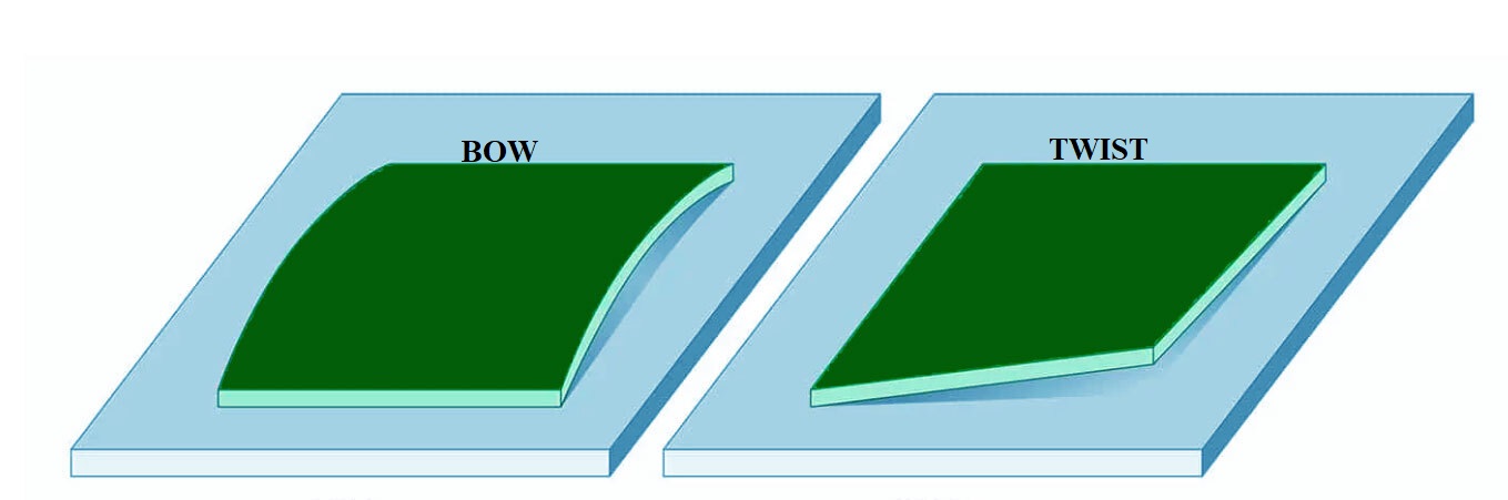
2. Bow
If copper coverage is not balanced, cylindrical or spherical curvature is formed on the PCB layer. In simple language, you can say the four corners of a table are fixed, and the top of the table rises above. It is known as a bow, which is a result of technical faults. The bow results in tension on the surface in the same direction as the curve. Further, it leads to random current flow across the board.

3. Twist
Twist is influenced by the board material and its thickness. It happens when any one corner of a board is not aligned with the others symmetrically. A particular surface diagonally rises up, then the other corners get twisted. This is similar to pulling up one corner of a mat on a table, causing the other corners to twist. Refer to the figure below.

4. Resin voids
This defect occurs due to improper copper distribution or plating. During assembly, pressure is applied in an asymmetric manner on the board. As pressure is a lateral force, the surface having a thin copper deposition oozes out resins. This creates voids in that location.
5. Failure to meet class 3 standards
The IPC class 3 is the highest and most stringent category among circuit board classes, requiring strict adherence to manufacturing specifications with minimal tolerance for defects. Unbalanced copper deposition beyond allowable limits can distort the circuitry, preventing the product from meeting these requirements.
To learn how to build reliable circuit boards, download the IPC Class 3 Design Guide.

IPC Class 3 Design Guide
8 Chapters - 23 Pages - 35 Minute ReadWhat's Inside:
- IPC guidelines for manufacturing defects
- IPC standards for assembly processes
- Common differences between the classes
- IPC documents to set the level of acceptance criteria
Download Now
How are bow and twist measured?
As per IPC-6012, the bow is calculated for a given PCB size as follows:
Bow allowance = (Board length or width x percentage of bow allowance) ∕ 100
Twist is calculated as:
Maximum allowable twist = (2 x Board diagonal length x percentage of twist allowance) ∕ 100
Twist measurement involves the diagonal length of the board. Since the board is constrained at one corner and twist occurs in two directions, a factor of 2 is included.
As per IPC-6012, the maximum allowable bow and twist is 0.75% for boards with SMT components and 1.5% for others.
Here, you can see the example of a board having a length and width of 4’’ and 3’’ respectively, and a diagonal length of 5’’.

For the above example, the bow and twist can be measured as:
Bow allowance across the length= (4 x 0.75) ∕ 100 = 0.03 inches
Bow allowance across the width= (3 x 0.75) ∕ 100 = 0.0225 inches
Maximum allowable twist = (2 x 5 x 0.75) ∕ 100 = 0.075 inches
Techniques for a balanced copper distribution
Hatch patterns, copper thieving, consistent trace placement, copper filling, and stack-up symmetry help achieve copper balance in boards.
1. Use hatch patterns in copper planes
Cross-hatching is a technique in which copper planes are patterned into a lattice structure with regularly spaced openings, resembling a mesh. The process creates small openings in the copper plane. These openings allow resin to flow through and bond more effectively with the laminate, improving adhesion and ensuring more uniform copper distribution. This helps reduce the risk of warpage and deformation.
The following are some benefits of hatched copper planes over solid pours:
- Enables controlled impedance routing in high-speed boards.
- Allows wider dimensions without compromising the flexibility of circuit assembly.
- Improves copper distribution under transmission lines, aiding impedance control.
- Provides mechanical support for dynamic or static flex boards.


2. Prefer thicker copper boards
Use thicker copper boards instead of thinner ones, if your design permits. The likelihood of bow and twist increases when thinner boards are used, as they lack sufficient material to maintain structural stiffness. Standard board thicknesses include 1 mm, 1.6 mm, and 1.8 mm. For boards thinner than 1 mm, the risk of warpage significantly increases compared to thicker boards.
3. Maintain uniform trace distribution across all layers
Conductor traces should be distributed uniformly across the board. Avoid copper nests wherever possible, as they can lead to uneven copper distribution. Ensure traces are placed symmetrically on each layer to maintain balance and reduce the risk of warpage.
4. Apply copper thieving in low-density areas
Copper thieving is a process of depositing non-conductive copper features to counterbalance the current flow in a PCB during the plating process. Current accumulation is higher in the areas where isolated traces are present. This causes under-etching of traces, resulting in a mushroom profile instead of smooth, squared edges.
This can be avoided by thieving, which redistributes excess current and balances the flow while plating the area where the metal is sparse. Moreover, variations in trace geometry impact the characteristic impedance and cause SI problems in the circuit.

Copper thieving involves adding small circles, squares, or even a solid plane of copper to large vacant spaces on the board. This helps distribute copper more evenly across the board. Special measures should be taken so that thieving does not make connections with any net and disturb the functionality of critical CI or RF traces.
4 benefits of implementing copper thieving
- Controlled finished thickness: Copper thieving enables you to balance the copper and dielectric percentages throughout the board surface. Due to this, you can achieve a consistent finished thickness.
- Even plating and etching: Another reward of copper thieving is accomplishing controlled etching/plating and uniform current distribution in a sparse zone.
- Reduced risk of outgassing, delamination, bow, and twist: Since the copper distribution is uniform, the chances of outgassing, delamination, bow, and twist are significantly less.
- Minimizes the need for excess etching: The etching process involves removing the excess copper to reveal the copper pattern with the help of a chemical solution. But if the etching solution gets saturated with copper, it becomes ineffective. Hence, the etching procedure has to be cycled again. Copper thieving decreases excessive etching and reduces the overall cost.
How can you implement copper thieving?
There are several design tools available that assist you in adding copper thieving automatically. You can specify the shape, size, and spacing of the pattern in your EDA tool. The shape doesn’t matter if copper is poured evenly throughout the board.
Copper thieving sometimes works as EMI shielding when incorporated in the form of a solid plane. It is essential to place this plane in the proper position and with correct spacing regulations. Otherwise, it may adversely impact the signal integrity of your design.
Why is copper thieving applied on outer layers?
Outer layers of the circuit board often have uneven copper distribution due to CI traces, component pads, and holes for press-fit connectors. If copper thieving is not applied, isolated features may receive more plating than denser areas, resulting in weak or unreliable connections. To avoid this, ensure sufficient copper is poured to support uniform plating of vias and component mounting holes.
When implementing copper thieving, you need to ensure that traces are not present below the pattern. This can adversely affect the impedance of those traces. To avoid this, clearly specify the requirement and accurate location of thieving in the fab drawing.
5. Fill open areas in each layer with copper
When a design requires large copper areas, the open regions should be filled with copper. This helps maintain balance with the corresponding opposite layer, ensuring symmetrical copper distribution across the stack-up.

6. Incorporate closely coupled power and ground planes
It is important to maintain uniform copper thickness across all signal and power planes. Power planes should also be symmetrical to ensure balanced performance.
During DesignCon, Heidi Barnes, the renowned senior applications engineer at Keysight, stated:
“One of the challenges is the power layers. The simplest form is to put the power and ground layers in the middle. If you can get the power and the ground closer together, the loop inductance is very much smaller, so the spreading inductance is less.”
7. Ensure prepreg and core symmetry in the stack-up
Maintaining symmetry in power planes alone is not sufficient to achieve uniform copper distribution. It is also essential to balance prepreg and core materials in terms of their placement and thickness within the stack-up.

Sierra Circuits fabricates and assembles high-quality circuit boards in the United States. Visit our PCB manufacturing capabilities to learn more.
What does copper weight mean in printed boards?
Fundamentally, copper weight is a measure of copper thickness on the board. It refers to the amount of copper distributed over one square foot area (oz/ft²) of a PCB layer. The standard copper weight we use is 1 oz or 1.37 mils. For example, if you are using 1 oz of copper for a 1 sq ft area, it corresponds to a thickness of approximately 1.37 mil.

The table below provides the copper thickness values in oz, mil, inches, mm, and µm.
| oz | 1 | 1.5 | 2 | 3 | 4 | 5 | 6 | 7 | 8 | 9 |
|---|---|---|---|---|---|---|---|---|---|---|
| mil | 1.37 | 2.06 | 2.74 | 4.11 | 5.48 | 6.85 | 8.22 | 9.59 | 10.96 | 12.33 |
| inch | 0.00137 | 0.00206 | 0.00274 | 0.00411 | 0.00548 | 0.00685 | 0.00822 | 0.00959 | 0.01096 | 0.01233 |
| mm | 0.0348 | 0.0522 | 0.0696 | 0.1044 | 0.1392 | 0.1740 | 0.2088 | 0.2436 | 0.2784 | 0.3132 |
| µm | 34.80 | 52.20 | 69.60 | 104.39 | 139.19 | 173.99 | 208.79 | 243.59 | 278.38 | 313.18 |
Copper weight is the critical factor that determines the current-carrying capacity of the board. If your design has high current or thermal requirements, you can modify the copper thickness. It also impacts trace resistance, heat dissipation, and overall reliability of the PCB.
What is heavy copper?
There is no generalized definition of heavy copper. Typically, 1 oz is considered the standard copper weight. However, if your design demands more than 3 oz, it is classified as heavy copper.
In general, higher copper weight increases the current-carrying capacity of a trace. It also enhances the thermal and mechanical stability of the board, making it more resistant to high current, elevated temperatures, and frequent thermal cycling conditions that can degrade standard PCB designs.
Additional advantages include:
- High power density.
- Greater capacity to hold several copper weights on the same layer.
- Increases heat dissipation.
Heavy copper boards are widely used in the following applications:
- Computer and automotive industries
- Military and industry control
- Power supply and distribution
- Power conversion
- Solar panel and welding equipment manufacturing
- Electrical vehicles with lithium batteries
When is light copper used in PCB design?
In some cases, you may need to reduce the copper weight to achieve a specific impedance. Since it is not always possible to adjust trace length and width, using a lower copper thickness becomes a practical solution.
You can use our trace width calculator to design the right traces for your boards.
How does copper weight affect trace spacing?
Higher copper thickness requires increased spacing between PCB traces.
The spacing between traces needs to be regulated when you use thick copper cladding. Different designers have different specifications for this.
Here is an example of the minimum space requirement with respect to copper weight.
| Copper weight | Space between copper features and minimum trace width |
|---|---|
| 1 oz | 3.5 mil (0.089mm) |
| 2 oz | 8 mil (0.203mm) |
| 3 oz | 10 mil (0.254mm) |
| 4 oz | 14 mil (0.355mm) |
What is the impact of copper weight on manufacturing cost?
As copper weight increases, the overall cost also rises. Naturally, the manufacturing time increases as well. The additional cost is not only due to the increased copper thickness but also includes higher shipping weight, quality assurance requirements, process complexity, and increased labor time.
For design for manufacturing strategies, download the DFM Handbook.

Design for Manufacturing Handbook
11 Chapters - 96 Pages - 90 Minute ReadWhat's Inside:
- Annular rings: avoid drill breakouts
- Vias: optimize your design
- Trace width and space: follow the best practices
- Solder mask and silkscreen: get the must-knows
Download Now
Sierra Circuits efficiently analyzes the suitability of heavy copper for a particular design. Based on DFM guidelines, our DFM engineers determine the appropriate etching time for heavy copper boards. As discussed earlier, balanced copper distribution can avoid warpage in the PCB. Typically, up to 0.7% warpage (of the board’s diagonal length) is permissible. Beyond this limit, the entire design may fail.
To prevent such issues, the manufacturing team carefully inspects copper distribution and ensures symmetrical build-ups.
If you have any questions regarding copper weight and balanced copper distribution, post your queries on our forum, SierraConnect. Our design and manufacturing experts will help you.
About Poulomi Ghosh : Poulomi is a microwave engineer specializing in EMI, EMC, RF, and high-speed electronics. As a senior technical writer at Sierra Circuits, she creates advanced engineering articles and webinars for hardware engineers and PCB designers.


