


Contents

On-demand webinar
How Good is My Shield? An Introduction to Transfer Impedance and Shielding Effectiveness
by Karen Burnham
PCB via filling is a technique in which the plated hole is filled with a conductive or non-conductive material. It enhances the reliability of the circuit board by reducing the possibility of air or liquid getting trapped.
In this article, you will learn the benefits, types, manufacturing process, and failure analysis of via filling.
Highlights:
- Choose Taiyo paste (non-conductive) for a balance between performance and affordability.
- Opt for AE3030 for high conductivity and reliable performance when cost is a secondary consideration.
- Refer to IPC-4761 standards for via filling and via covering.
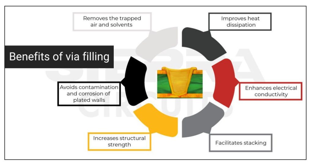
What is the purpose of via filling?
A via is a copper-plated hole that creates an electric connection between different layers of a PCB. Normally, any type of via, such as through-hole, microvia, blind, and buried, can be filled. First, the hole wall is plated to make it conductive. Later, the barrel is filled with conductive (copper) or non-conductive (resin) material.
The purpose of filling vias is to:
- Avoid the entry of any impurities. Hence, there is a lower chance of contamination or corrosion
- Improve the mechanical strength of vias and pads
- Place SMT components on the via hole (only if it is resin-filled)
- Strengthen the pad attachment
- Reduce the risk of solder wicking
- Prevent the trimming of the silkscreen printing
- Enhance the thermal conductivity and current capacity of a via (if it is conductive filled)
While the via-filling procedure can be intricate, the benefits far exceed the complexity. At Sierra Circuits, we approximately fill 30,000,000 holes every month.
What are the types of via filling?
You need to carefully consider the choice of via-filling as it impacts the board’s cost and production time.
Conductive polymer filling
Conductive materials like copper or silver epoxy are used to fill the holes. These metals aid in effectively transferring the electric signal and improve the thermal conductivity of the via. The conductive filling can also help to divert the heat from large components like ICs, BGAs, microcontrollers, and processors.
Copper epoxy has better thermal conductivity, but silver epoxy is more cost-effective.
Compared to non-conductive filling, conductive polymer filling can be expensive. However, it can create a perfect plating of via walls without any voids. This can significantly improve the current flow between the inner layers.
Non-conductive via plugging
This does not improve the electrical or thermal conductivity of the via. It provides structural support to the pad in case of a via-in pad. During the PCB manufacturing process, the epoxy paste or resin is filled into regular vias. The walls are still plated with copper for electrical connectivity. It is important to avoid voids in the plating as they can create connectivity issues.

For expert design for manufacturing guidelines, download our DFM handbook. This e-book helps you identify potential manufacturing errors during the design phase and ensure the manufacturability of your board without design iterations.

Design for Manufacturing Handbook
11 Chapters - 96 Pages - 90 Minute ReadWhat's Inside:
- Annular rings: avoid drill breakouts
- Vias: optimize your design
- Trace width and space: follow the best practices
- Solder mask and silkscreen: get the must-knows
Download Now
Cost considerations for conductive and non-conductive PCB via filling
Via filling requires additional steps such as electroplating and filling to deposit the conductive or non-conductive material inside the via holes. This adds to the overall cost of the circuit board.
4 factors that affect the via-filling cost
1. Hole count
The number of vias or through-holes in a PCB directly impacts the filling cost. More holes generally mean more paste is required, leading to higher material costs and increased processing time.
2. Type of paste
The choice of paste can significantly impact the overall cost of the hole-filling process. Here are a few commonly used pastes:
- Taiyo paste: It is a non-conductive and cost-effective paste. It is a popular choice for manufacturers looking for a balance between performance and affordability.
- San E Fill: This via plugging paste shares similar characteristics with Taiyo in terms of being non-conductive.
- AE3030 (conductive) paste: It is likely chosen when high conductivity and performance are critical. This paste is slightly expensive when compared to the previous filling materials.
3. Manufacturing complexity
Conductive via filling typically involves several sequential steps, including activation, electroless copper deposition, a time-consuming electroplating process, and chemical mechanical polishing (CMP). Certain steps in conductive via filling may also involve curing or drying processes.
Further, each of these steps adds complexity to the process and requires careful control and monitoring, eventually increasing the manufacturing time.
In contrast, non-conductive via plugging processes, which involve filling vias with insulating materials like epoxy resins, are generally simpler and are often less time-intensive than the processes involved in depositing and solidifying conductive materials.
4. Testing and quality control
Conductive-filled vias may require additional testing to ensure proper electrical conductivity. This testing adds to quality control costs.
Non-conductive via plugging primarily involves ensuring proper insulation between layers. Testing requirements for non-conductive via plugging are less stringent compared to conductive via filling.
Alternative budget-friendly via-filling techniques
An alternative method to fill vias with paste is using a via-fill plug. This involves applying a liquid photo-imageable (LPI) solder mask over the entire surface of the PCB, covering the drilled vias as well. The mask is then exposed to ultraviolet light through a photo-imageable process, which allows for selective curing to create a solid plug.
Customers can request this process, which may offer a different set of advantages and disadvantages compared to traditional via filling.
Advantages of via fill plug with LPI solder mask
- This method can be more cost-effective compared to traditional via-filling processes involving materials like copper paste or epoxy resins.
- The via-fill plug using LPI solder mask is a simpler process as it eliminates the need for complex electroplating or epoxy-filling steps.
- The photo-imageable process allows for selective curing of the solder mask, enabling precise via filling without affecting other parts of the board. Hence, this method is suitable for applications requiring smaller hole sizes.
- LPI solder mask materials exhibit good thermal conductivity, contributing to improved thermal performance of the vias.
Disadvantages of the via fill plug with LPI solder mask
- While LPI solder mask materials may have some electrical conductivity, it is not as high as conductive materials like copper. This makes it less suitable for applications with stringent conductivity requirements.
- The choice of materials for the via-fill plug is limited to those compatible with the LPI solder mask process.
- The process relies on accurate UV exposure during the photo-imaging step, and any deviations can impact the quality of the via-fill plug.
Reducing via fill costs in high-volume productions
The strategies available to minimize filling costs in high-volume PCB production are limited. High-volume production often relies on standardized processes to ensure repeatability and efficiency, limiting the ability to implement highly customized hole-filling techniques.
The primary options involve changing the fill requirements, such as using a via-fill plug or employing plate shut techniques.
Via fill plug
The via-fill plug technique employs a plug made of materials like epoxy resins, applied over vias to create a solid fill. This technique reduces the number of individual vias that need to be filled, streamlining the process and potentially lowering costs. It is beneficial in applications where insulation is the primary requirement and electrical conductivity in the vias is not critical.
Plate shut
This method modifies the design by closing or shutting unused vias during manufacturing, eliminating the need for filling. This simplifies the manufacturing process and is effective when specific vias are unnecessary for the application or if there is an alternative routing option available. You need to ensure the closed vias do not impact the functionality or performance of the PCB.
Fab notes for via filling
- Always mention the type of via fill (conductive or non-conductive).
- The CTE values of the via filling and dielectric material should be equivalent to avoid stress fractures due to expansion.
- Plating thickness and via-in-pad specification, if any.
IPC 4761 standards for via filling and via covering
Via covering and filling benchmarks are depicted in the IPC 4761 standards. In this section, you will learn about the 12 standards defined in the document.
Type I (a): Via is tented on a single side using solder mask. There is no protection for the hole walls on the other side. It can also have long-term reliability issues.
 via")
Type I (b): The hole is tented on both sides with a solder mask. This type of via covering can have dimples on the surface.
 via tenting")
Type II (a): Here, the via is covered with a second mask layer on a single side.
 via tenting")
Type II (b): The via is tented and covered with a secondary mask on both sides.
 via tenting")
To know more about the via tenting process and its design rules, read PCB via tenting design rules and fabrication notes.
Type III (a): The via is partially filled or plugged with liquid photo imageable (LPI) solder mask or resin material. Here, the material can protrude from the other side.
 via plugging")
Type III (b): The LPI solder mask or resin plugs both ends of the via. This can cause the air or the solvent to be trapped in the middle, which can blow out during the curing process. The mask can also cover the annular ring and affect connectivity.
 via plugging")
Type IV (a): In this type, the via is plugged and covered with a resin/solder mask on one side. The additional mask layer strengthens the plug.
 via plugging")
Type IV (b): The via is plugged and covered on both sides with a solder mask.
 via")
Type V: The via is completely filled with conductive or non-conductive material. This avoids the contamination of the copper walls. Planarization of the surface is required if you opt for this type of filling.

Type VI (a): The via is completely filled and covered with an LPI solder mask on one side. It reduces the risk of voids on the surface of the filled hole.
 via filling")
Type VI (b): Here, the via is completely filled, and the solder mask covers both sides of the plated hole.
 via filling")
Type VII: The filled via is capped with a secondary metalized coating on both sides. This is mostly used to fill via-in-pads and stacked microvias in HDI boards. Here, the filled via is capped with a secondary metalized coating on both sides,
Creating a strong adhesion between the metal coating, filling, and copper pad can be an issue. If the via is not filled or the metal coating is thin, it can cause dimples on the surface. The air trapped in the dimples can cause issues during PCB assembly.

All of the above via types have their own drawbacks. Always consider your manufacturer’s recommendations before deciding on the type. Type-VII is popularly used in via-in-pad and HDI boards with stacked microvias. Here, the filled via is capped with a secondary metalized coating on both sides.

How do you fill vias during PCB manufacturing?
Filled vias are processed before creating other metalized through-holes to make sure only the desired drills are filled. Before this process, the board will be cleaned to eliminate contamination. Below are the manufacturing steps :
Drilling: The vias that need to be filled are drilled first. While drilling, it is also essential that the drill penetrates and exposes the bottom layer or target pad. The hole can be drilled with either mechanical or laser drilling. For more, read PCB drilling explained: the dos and the don’ts.

The choice of equipment is based on cost, volume of production, precision, hole depth, and diameter. It is also important to consider that mechanical drills have the risk of drill wander. Additionally, ensuring the right hole size and aspect ratio is also important.
Cleaning: The heat generated during the drilling process causes the resin to smear on the copper features of the hole. Furthermore, it also leaves burrs on the edge of the via and other residues. Hence, the drilled hole is cleaned using a brush and solvents. Later, it goes through a de-smearing process.

Preparation for plating: For electroplating, it is essential to have a conductive copper layer inside via holes, since they also contain fiberglass. This can be achieved using traditional electroless plating or the black hole process.

Plating: A photoresist creates the image of via holes that require filling. The photoresist over the via is removed after development so that only the desired are exposed. Now, using the electroplating process, via walls are plated with copper. Next, the complete photoresist layer is removed and baked to remove the moisture.

Filling with resin: After plating, vias are ready to be filled with resin. Pressure and vacuum are applied during the filling process to prevent any voids in the hole barrel. The excess resin is removed from the board and baked to harden.

Planarization: After curing, the filled resins can have bumps. Hence, a machine with mechanical brushes removes the excess resin and creates a uniform surface. This is called planarization. This facilitates a smooth over-plating process, which is essential for soldering components.
The above-mentioned manufacturing steps are additional and only required if your design has a filled via. Hence, this can increase the cost of production. You can fill only a few vias in your circuit instead of all of them. This approach will lower manufacturing costs and simplify the overall design.
Filling of via-in-pad
Filled and capped vias are also used as via-in-pad solutions. Here, the hole is placed on the component pad, as shown in the image below. This will make the signal path much shorter when compared to the traditional dog bone structure. If the via is not placed on the pad then there is no need for a filling. An extra plating step is required to cap the filled via. Hence, this can further increase the cost and turnaround time of your PCB.

Filling of microvias in HDI boards
Filling and plating the microvia is done in a special plating tank. It plates the laser-drilled hole from bottom to top until the hole is completely filled. Always plate stacked vias and vias-in-pad to improve reliability. For staggered vias the holes need to be closed as the resin can seep into the hole during the lamination process.

Download the HDI PCB Design Guide for guidelines on designing high-density circuit boards. This e-book will help you plan your stack-up with microvia structure, choose the right materials, and manage signal integrity and controlled impedance requirements.

HDI PCB Design Guide
5 Chapters - 52 Pages - 60 Minute ReadWhat's Inside:
- Planning your stack-up and microvia structure
- Choosing the right materials
- Signal integrity and controlled impedance in HDI
- Manufacturing considerations for higher yields
Download Now
Failure analysis of filled vias
Many factors can cause the failure of a filled via, such as large dimples, leakage, and a void inside. Hence, each element has to be analyzed for potential failures and resolved. Below are a few reasons for filled via failures.

Fractures in the via wall create an electrical discontinuity
The general reason for failure is barrel stress. This causes cracking of the via plating, which can cause connectivity issues. The stress in the hole walls can be avoided by plating a thicker copper layer.
Void in filled vias cause reliability issues
Trapped air inside the barrel is another reason for failure. In the cleaning step, remove all the air. Using a solvent with lower surface tension can help.
Voids can cause reliability issues and reduce the lifespan of the via. The impact of a void depends on its size, shape, and location. Small and spherical gaps cause fewer issues when compared to large gaps. IPC 6012 standard depicts the guidelines for the acceptable voids present in the via, barrel fill, and plating.
- For class 2 boards, 1 void is allowed per hole. It should not exceed 5% of the hole. 75% of barrel fill is essential for through-hole leads. Class 2 permits 50% fill under specific exceptions.
- For class 3 boards, no void is allowed. 75% of the barrel must be filled. See IPC class 2 vs class 3: the different design rules for more details.

Environmental impurities can result in voids
With many types of equipment, materials, and chemicals used in the production environment, it is difficult to remove all the pollutants. The microparticles that are not visible to our naked eye can end up in the via barrel. This will create a void during the filling process and eventually result in the failure of a via.
The following steps can help avoid impurities:
- Enclose the production line to reduce the risk of debris
- Ensure that all the materials used are of top quality
- Filter the plating agents regularly to maintain their vividness and purity
An imbalanced plating process can cause voids
Voids can occur when the plating rate is not uniform. The imbalance of leveling agents and poor solution agitation are the main reasons for this. Ensuring the right proportions of the plating chemicals and periodically checking the condition of the solutions will reduce voids.
Our engineers prioritize performance, manufacturability, cost, and design for testability to ensure the best possible board at a fair price. Check out PCB design services to learn more.

Key takeaways:
- Conductive and non-conductive are the two types of via filling, each with its advantages and cost considerations.
- The purpose of via filling includes avoiding impurities, improving mechanical strength, allowing for the placement of SMT components, strengthening pad attachment, reducing solder-wicking, preventing silkscreen printing issues, and enhancing thermal conductivity and current capacity.
- The cost of via filling depends on the hole count, the type of paste used, the complexity of the manufacturing process, and the testing and quality control requirements.
- Alternative techniques, like via fill plug with LPI solder mask, offer cost advantages over traditional methods.
- High-volume production considerations include using via fill plug or plate shut techniques to reduce costs.
- The filling process during PCB manufacturing involves drilling, cleaning, preparation for plating, electroplating, filling with resin, and planarization.
- To shorten signal paths, use filled and capped vias as via-in pads instead of the traditional dog bone structure. The additional plating step for capping impacts the PCB’s cost and turnaround time.
- Failure analysis of filled vias includes issues like barrel stress, voids, environmental impurities, and an imbalanced plating process.
Filling vias can improve their electrical conductivity, mechanical strength, and thermal dissipation in PCBs. Based on your design and cost constraints, you can choose a suitable via fill. It is also important to find a manufacturer who can build vias as per your requirements.
If you need any assistance in designing your vias, post your queries on our PCB forum, SierraConnect. Our manufacturing and design experts will be happy to help you.

About Sushmitha V : Sushmitha V has a master's degree in power electronics and has over four years of experience in the PCB industry. Her areas of interest include circuit board manufacturing, assembly, IPC standards, and DFM/DFA practices.


Start the discussion at sierraconnect.protoexpress.com