What is PCB assembly?
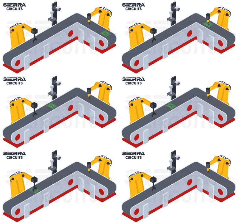
PCB assembly is the process of populating a circuit board with all the desired components. It involves DFA, SMT, and through-hole components placement, testing, and final inspection.
To ensure an efficient assembly process, you need to provide a clean BOM and assembly notes with all the necessary callouts, such as reference designators, component orientation, and instructions related to washable and non-washable parts.
Here you’ll learn the step-by-step circuit board assembly process and the best practices for component selection.
Step-by-step PCB assembly process
The fab house crafts the circuit boards according to the DFM guidelines before they reach the assembly house. Adhering to the DFM benchmarks is crucial to avoid potential manufacturing errors such as insufficient trace spacing and copper slivers.
After fabricating the boards, the fab house sends them to the assembly facility.
The flowchart below illustrates the stages involved in board assembly.
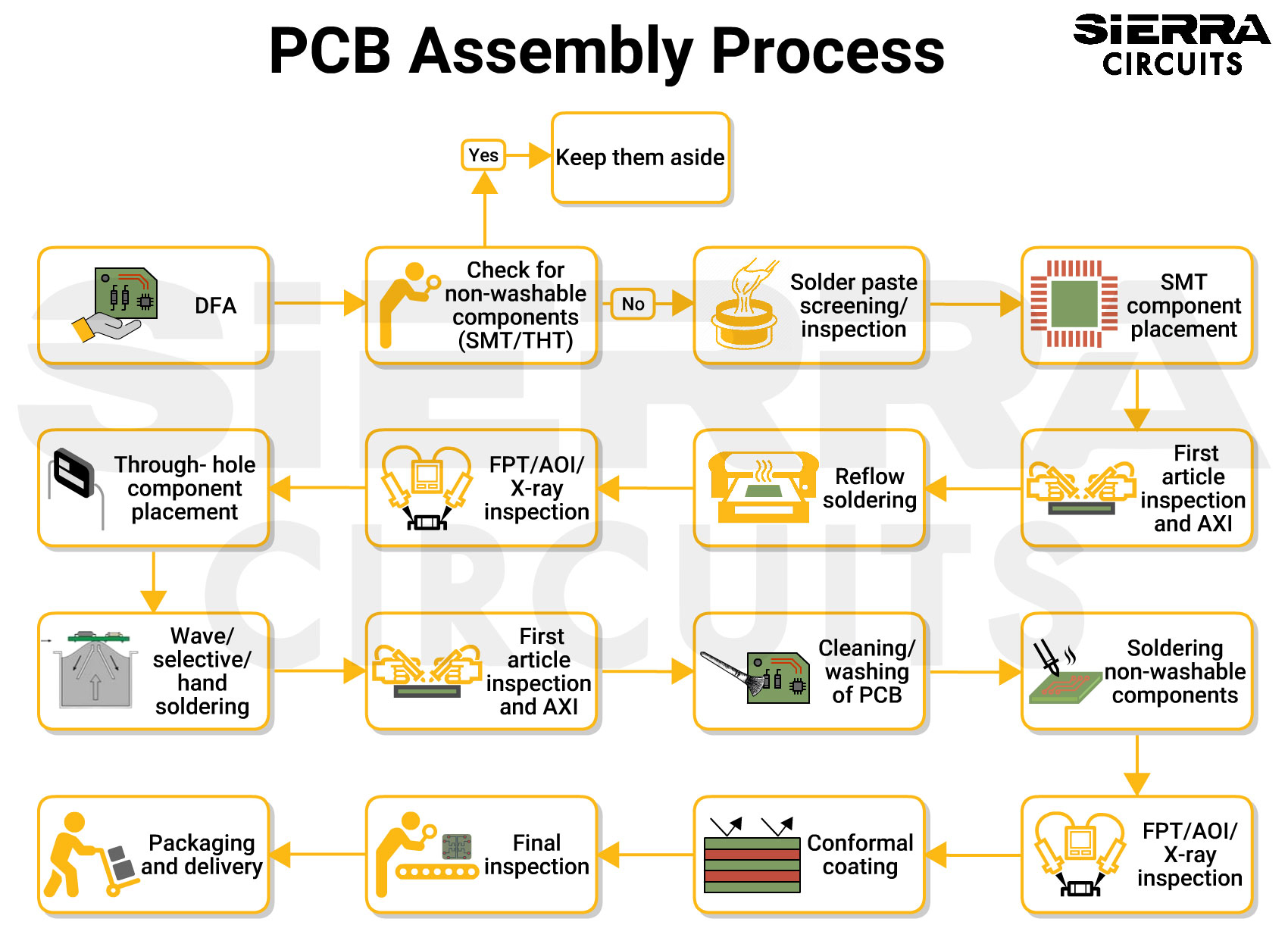
1. DFA: Verifies Gerber/ODB++ and BOM
Design for assembly is the first stage of PCBA. During this stage, DFA engineers verify the data present in the Gerber/ODB++ and circuit board BOM files.
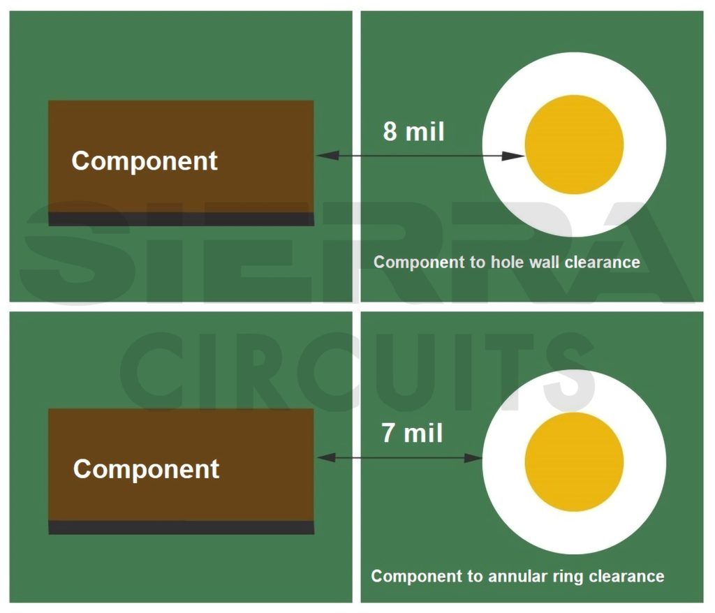
As a designer, you should always follow the DFA guidelines to avoid board respins. The primary objective of this step is to avoid potential assembly errors and reduce the overall cost of your board. DFA engineers ensure:
- Correct implementation of the parts listed in the BOM
- Component footprint dimensions are accurate
- Adequate spacing between the components
- Drill file specifications are followed
- Incorporation of adequate circuit board thermal relief techniques
- Board edge clearance rules are in compliance
After verifying these parameters, we begin with the SMT assembly.
Design for Assembly Handbook
6 Chapters - 50 Pages - 70 Minute ReadWhat's Inside:
- Recommended layout for components
- Common PCB assembly defects
- Factors that impact the cost of the PCB assembly, including:
- Component packages
- Board assembly volumes
Download Now
2. SMT assembly process using pick and place machine
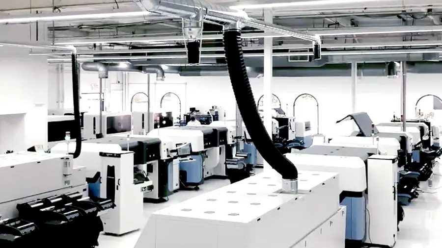
SMT assembly involves placing and soldering electronic components to the board using an automated system called the pick and place machine.
Before mounting the SMDs, the assembly house checks if there are any non-washable components. If they are present, we will assemble them at a later stage (after washing the circuit board). Surface mount assembly involves the following steps:
a. Solder paste screening/inspection
In this step, we will apply solder paste uniformly using stencils. Solder paste is a combination of powdered metal solder, like tin, silver, and copper, and a flux medium.
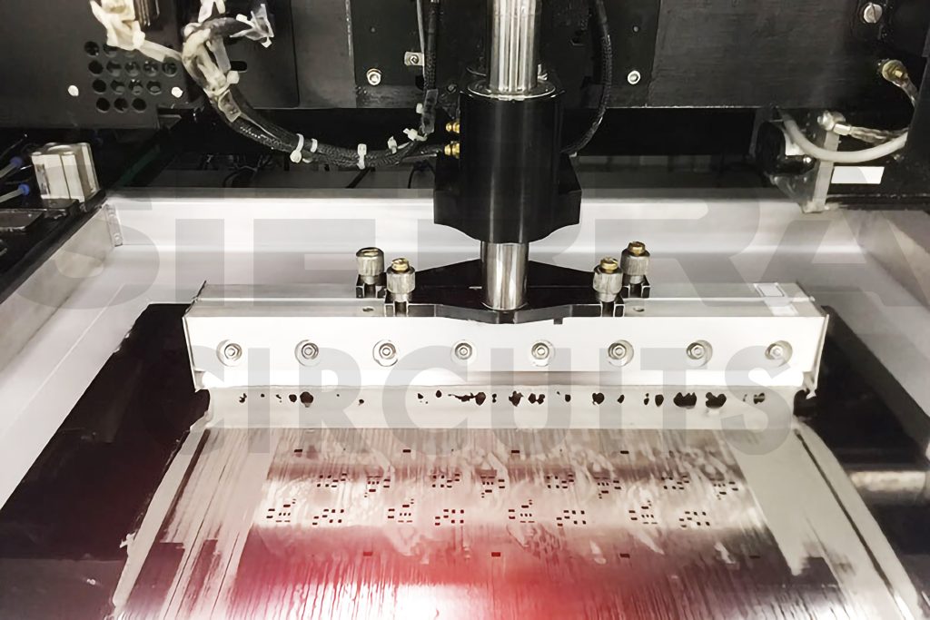
Our assembly experts apply the solder paste using an SMD stencil. An SMD stencil is a thin sheet of material (usually stainless steel) with a series of apertures that resemble the component pads on the board. The stencil accurately deposits the right amount of paste on the surface mount pads.
If you would like your CM to use any specific solder paste, you can call out the same in your PCB assembly notes.
After applying the solder paste, we inspect the paste with the help of solder paste inspection (SPI) machines. There are two types of SPI devices: 2D and 3D.
2D equipment can measure the height and width of solder paste deposits. 3D machines can calculate the length, width, and volume of the applied solder paste. These devices can also detect assembly errors such as missing paste and solder bridges.
b. SMT component placement

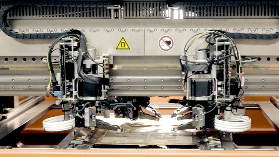
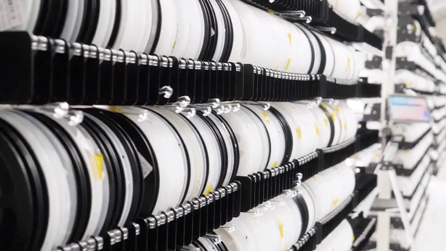
After applying the solder paste, a pick and place machine mounts components such as BGAs, ICs, resistors, and capacitors. This device picks a component from a tape, rotates it to the desired orientation, and places the part on the board.
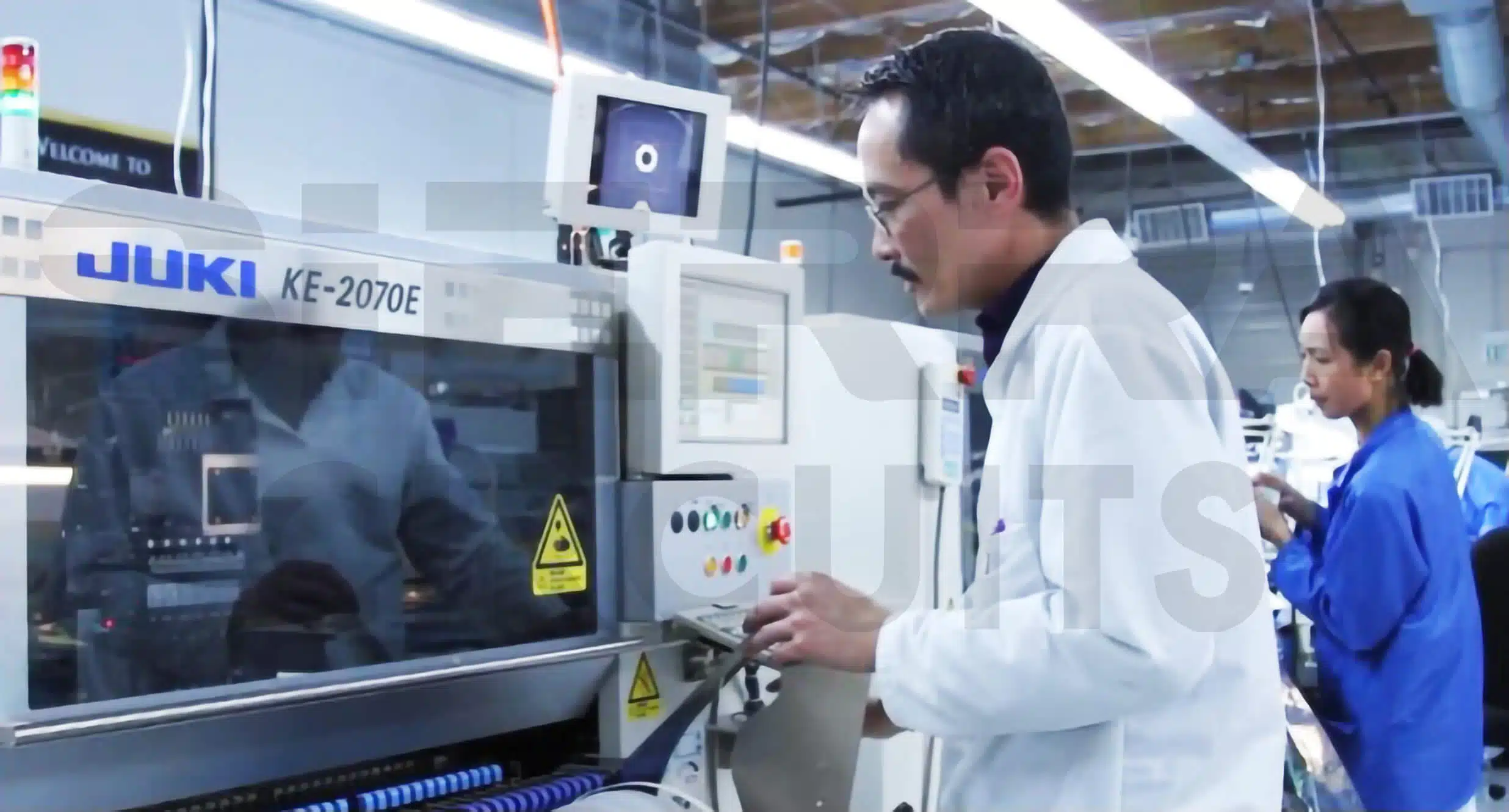
Sierra Circuits implements advanced Juki machines that can place up to 15000 components per hour. This enables us to assemble your prototypes with a 24-hour turnaround time
c. Reflow soldering
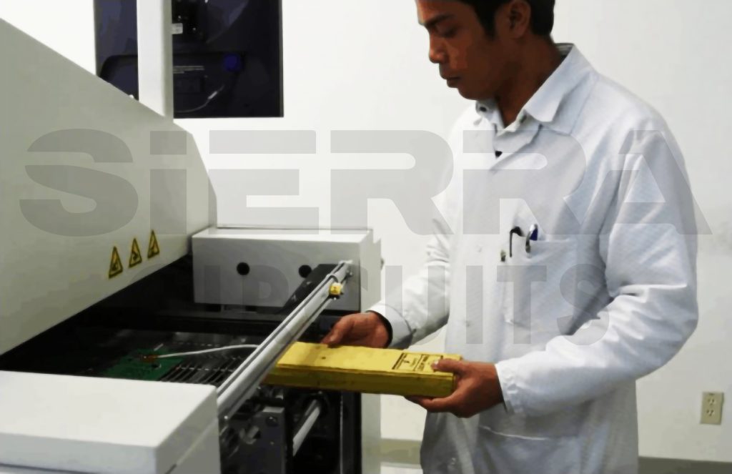
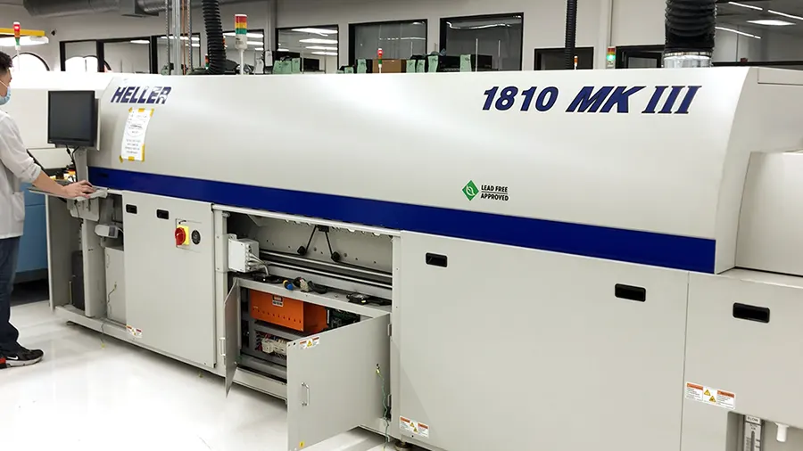
Reflow soldering is conducted only for SMT assembly (wave soldering for through-hole components will be discussed later). The circuit board, along with the mounted components, passes through the reflow oven. In this stage, the solder paste melts and establishes a solid connection between the components and their pads upon cooling. The components are rigidly fixed to the board.
The temperature range of reflow soldering depends on the type of solder paste used. 180-220°C for lead solder paste and 210-250°C for lead-free solder paste.
d. Automated optical inspection (AOI)
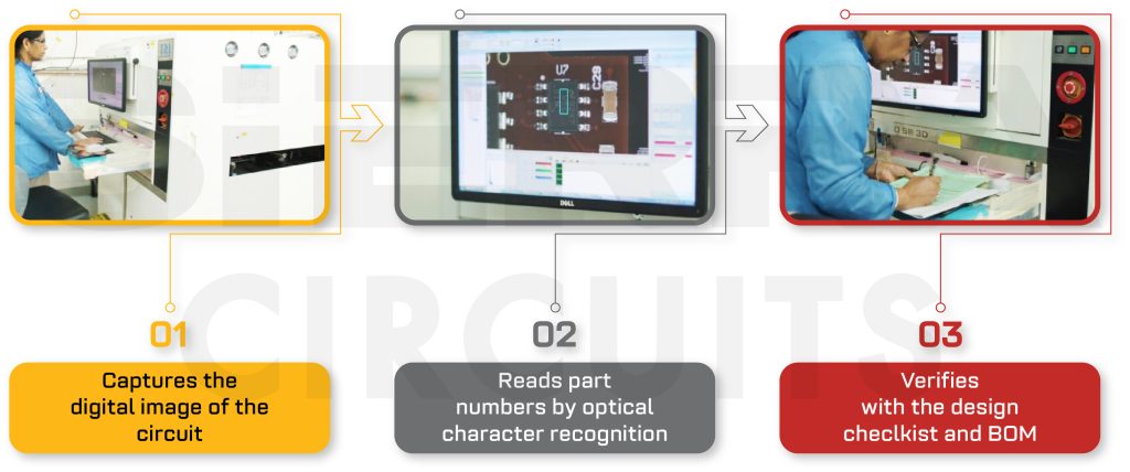
AOI systems use optical devices to automatically inspect the solder joints and components on the PCB for defects. They identify flaws such as missing components, solder difficulties, misalignments, wrong component orientation, lifted and misplaced components, open circuits, solder shorts, and insufficient or excess solder. This process aids in quality assurance.
e. X-ray inspection
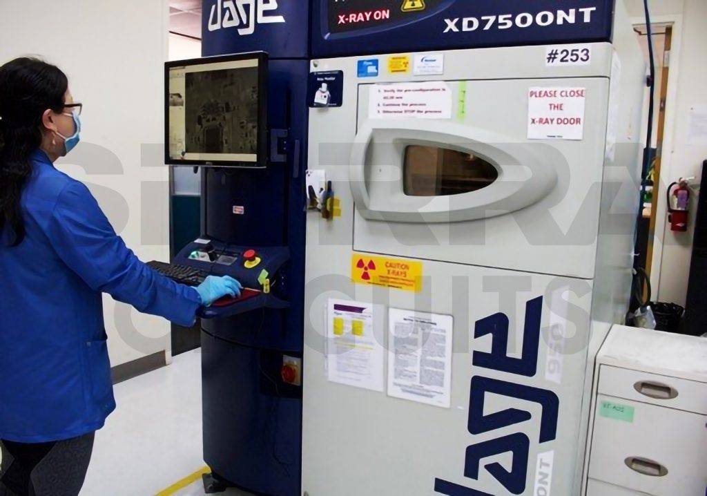
X-ray inspection is a non-destructive testing (NDT) method that makes use of X-rays to create images of the internal structures of an object. This method is used for multilayer and complex circuit boards with fine-pitch components. It reveals any defects in the internal solder joints of the board.
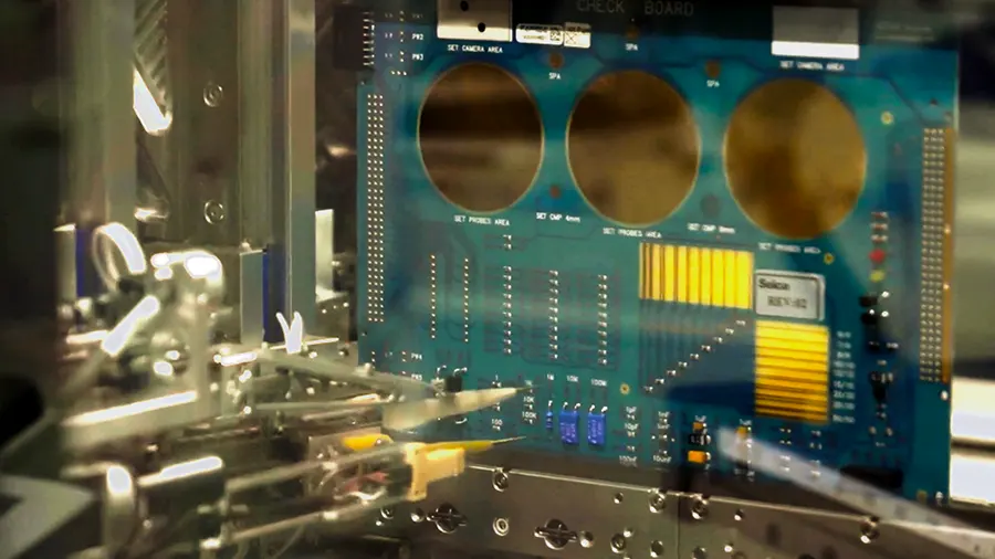
f. Flying probe testing (FPT)
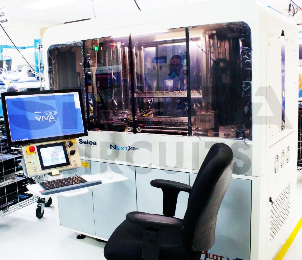
FPT is an automated PCB testing method that detects shorts, opens, and component attributes such as resistance, capacitance, and inductance. The testers consist of multiple movable test probes (typically two or more) that can move freely in X, Y, and Z directions over the surface of the board.
This makes the probe highly flexible and efficient for small production batches and frequent design changes.
The flying probe tester is programmed with the netlist information taken from the design files during the testing phase.
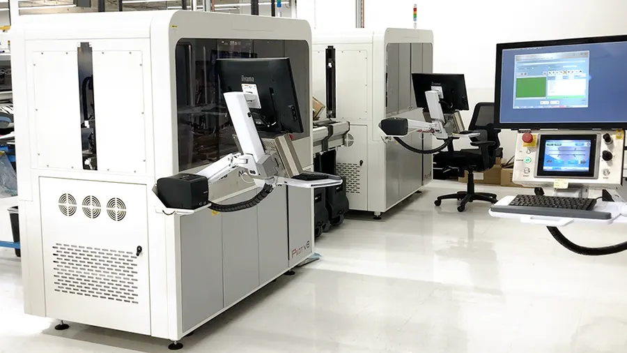
To measure the electrical properties of the circuit, such as resistance, capacitance, and continuity, the tester then moves the probes to various testing locations on the PCB. Sierra Circuits is equipped with Seica Spa Pilot V8 machines for flying probe testing.
At this stage, the SMT assembly process is completed. Further, through-hole components are examined and checked for non-washable components. If present, just like surface-mounted non-washable components, they are also kept away and soldered after cleaning.
Design for Testing Handbook
7 Chapters - 28 Pages - 45 Minute ReadWhat's Inside:
- PCB testing strategies
- Guidelines to design and place a test point for FPT
- Directives to make your board ICT compatible
- Benefits and drawbacks of various testing methods
- Defects that you can identify through board testing
Download Now
3. Through-hole assembly
Through-hole part insertion can be carried out manually or by automated machines. There are three types of soldering techniques used for through-hole assembly.
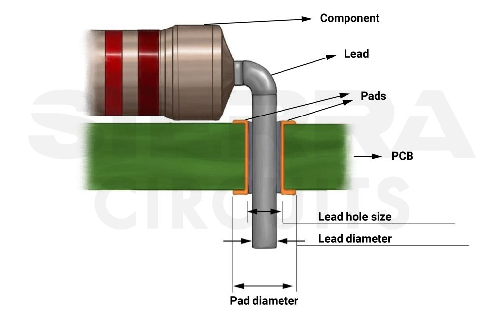
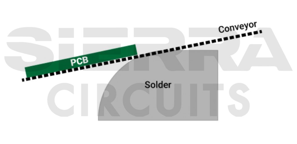
Wave soldering: This technique is carried out for large-scale soldering processes. Here, the parts are placed on the board, and liquid flux is applied to the component leads. Next, the board is preheated to a specific temperature and passed through a solder wave using a conveyor to create solder joints.
Selective soldering: It involves applying solder to a particular through-hole location on the circuit board using robotic soldering equipment or a special solder nozzle. The equipment consists of a flux spray, soldering pot, and solder head feeder. The solder head moves into position so that it can solder from underneath. This method is quicker and repeatable when compared to manual soldering.
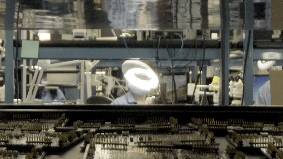
Hand soldering: It is a manual soldering technique used to attach components to a printed board using soldering equipment and wire. In this procedure, we use flux to clean the metal surfaces. This prevents oxidation from happening while hand soldering.
If there are any sensitive through-hole components in your design, you can choose a specific soldering method to assemble them. Clearly mention this in your PCB assembly notes.
4. Cleaning of assembled boards
After mounting the components, the team cleans the board using deionized water or a kaizen solution to remove flux residues and contaminants. They treat the circuit board with deionized water jets at high temperatures and pressures
We maintain the water temperature at 144°F while applying a pressure of 45 pounds per square inch. After washing, they dry the circuit board in the air using powered air jets.
5. Soldering of non-washable components
If there are any non-washable components in the design, they are soldered to the board at this stage. No-clean flux is generally used to solder these parts. This type of flux doesn’t need to be cleaned up after the soldering procedure.
This flux has resins and activators that are used to make the solder flow more easily and less likely to oxidize.
We perform AOI, X-ray inspection, and FPT after assembling these components.
6. Final inspection and testing
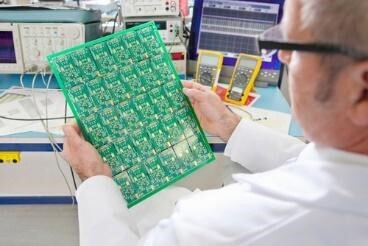
After completing the PCB assembly, the team sends the board for the final inspection. Next, we perform a quality inspection to check for physical and electrical flaws, such as missing components, solder defects, open circuits, short circuits, and incorrect component values.
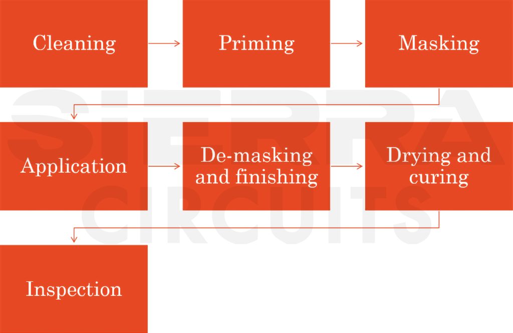
7. Conformal coating
Conformal coating is applied to a circuit board to create a barrier between contaminants and the PCB. It also creates an insulating layer, reducing crosstalk, leakage current, and electrochemical migration in the board. The coating material consists of acrylics, polyurethanes, silicons, epoxy, or a combination of resins.
The block diagram below shows the steps involved in conformal coating.
The most reliable PCB assembly in Silicon Valley
Avoid component procurement delays by using a single vendor to source your parts. Transparent pricing. Fast turn-times.
Learn more about our assembly services here.
Key takeaways:
- PCB assembly process involves DFA, SMD assembly, solder paste application/inspection, reflow soldering, board cleaning, through-hole component assembly, soldering non-washable components, circuit board testing, and final inspection.
- Always provide a clean BOM and detailed assembly notes to ensure a smooth assembly process.
- Your assembly notes should clearly mention the solder paste recommendations, cleaning component placement, and soldering instructions.
- If there are any sensitive through-hole components in your board, clearly provide instructions on how to handle those parts. For instance, the wave soldering process may damage some THT parts. In such cases, you need to ask your assembler to manually solder these components.
Get started with printed circuit board assembly
Sierra Circuits is capable of assembling BGA, micro-BGA, QFN, and other leadless package parts. Whether you need 1 or 10,000 boards assembled, we make it easy for your project to come to life.
3 tips for choosing components for your PCBA
As a designer, you need to make some key decisions about the type of components used in your board. Stick to these guidelines while choosing parts for your board assembly.
1. Procure components from a reliable supplier
Sourcing all the components from a reputable manufacturer reduces the risk of counterfeit or damaged parts. You can avoid part procurement hassles by opting for PCB component management services. Here, your fabricator will procure reliable parts from verified suppliers.
2. Opt for IC packages to reduce the part count
Component packages integrate several parts into a single enclosure to perform a desired function. For instance, a basic filter circuit consists of a resistor and a capacitor. If you opt for a package that functions as a filter, you can minimize the number of components used on your board. This results in improved reliability, reduced weight, and cost of your board.
3. Select SMT components as much as possible
SMT components have shorter leads when compared to through-hole parts. This reduces the parasitic capacitance and enhances signal integrity. Other benefits of choosing SMDs are:
- Less maintenance
- Make boards smaller and lighter
- Placing SMT components on both sides of a PCB allows for more design flexibility
- Easier to automate assembly compared to THT components
- Reduced manufacturing costs
For more, read advantages and disadvantages of surface mount technology.
Choose THT components only in special cases where the component required is not available, and SMD is particularly sensitive to temperature.
Key takeaways:
- Always procure components from a reliable supplier to avoid the risk of counterfeit parts
- Implement component packages to reduce the part count and size of the board
- Use small lead SMT components to enhance the signal integrity
Sierra Circuits PCB assembly services with rapid turnaround time
Sierra Circuits offers a wide range of circuit board assembly services – SMT, BGA, THT, mixed, and rigid-flex PCB assembly – tailored to your unique specs.
Whether you need a full turnkey, consigned, or partially consigned board assembly, we cater to all of your requirements.
Our PCB assembly services meet all the industry standards, such as IPC-A-600, IPC-6012, AS9100D, ISO 9001: 2015, and ISO 13485:2016.
Full turnkey PCBs
For turnkey orders, we handle the entire circuit board manufacturing and assembly process. We source and stock components from a reliable manufacturer. This enables us to provide full turnkey prototypes with a 24-hour turnaround time.
Partially consigned assembly/COIN services
In this order, you have the option to provide some of the parts while we take care of the rest. Here, you will get a personalized PCB component stocking service called customer-owned inventory (COIN). This enables you to mitigate supply risks by ensuring elusive components are readily available before the assembly process.
To overcome counterfeit and low-quality parts, opt for COIN services wherein we procure, store, and manage your components.
Check out our FAQs on COIN services.
Consigned assembly
This order allows you to provide all the components required for your board assembly. Our skilled assembly experts will populate your PCB to the highest quality standards. Follow the kitting guidelines for consigned assembly.
Knowledge of the step-by-step circuit board assembly process enables you to optimize your design. Always follow the DFA guidelines during the design phase to ensure error-free PCBAs. Choose components that are readily available to reduce the supply chain risks and time-to-market.
