


Contents

On-demand webinar
How Good is My Shield? An Introduction to Transfer Impedance and Shielding Effectiveness
by Karen Burnham
Designing with PCB assembly in mind is one of the most important and frequently misunderstood elements. This series is dedicated to helping you become a designing pro—someone whose board design has been optimized on the first try, ensuring a smooth, quick-turn production process.
Follow these tips when you design for assembly.
What is PCB design for assembly (DFA)?
Before going any further, let’s discuss what board assembly entails. After a board design is submitted and approved, be it flex, high-density interconnect (HDI), or otherwise, it is fabricated. Once that is complete, the bare boards will need to be assembled with additional components, including processors and memory.
Simple enough. The problem that often emerges—at least among those who are not yet PCB Masters—is that the initial circuit board design does not fully take assembly into account.
Instead, they focus exclusively on the board itself without a broader context of how the board will be used within the product or application.
Overlooking board assembly can lead to significant complications. A circuit board design may seem perfectly acceptable when viewed in isolation, but certain design decisions may make assembly difficult later on.
For example, components may be situated too close to one another, which could lead to a non-functioning product or cause performance issues. We’ll discuss this in-depth later in the article.
Then, there’s also the question of component availability. For the circuit board assembly process to flow smoothly—and, therefore, for the board production as a whole to progress effectively—the assembly vendor needs to have the requisite components on hand as soon as the boards arrive.
If they aren’t available, the whole process will be delayed, undermining the value of a quick-turn approach to board production.
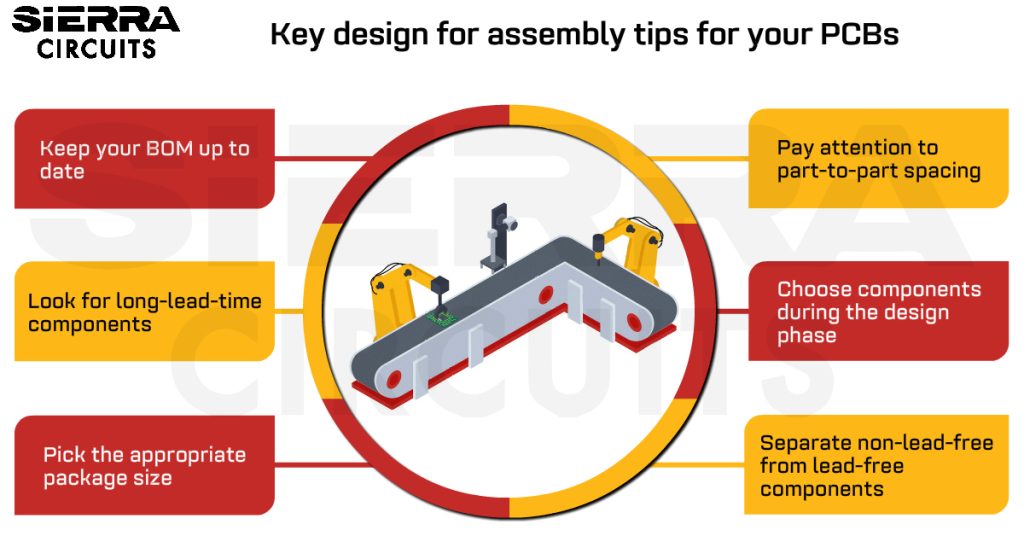
The illustration below shows 5 critical DFA norms every PCB designer should know.

14 DFA tips
The aforementioned issues may arise if you aren’t considering the assembly requirements during the design phase. Here are the key things to consider for PCB assembly.
1. Pay attention to part-to-part spacing
One of the frequently asked questions posed by designers who are not yet board masters is regarding component-to-component spacing.
Placing a component too close to another component can create various issues that may require re-design and re-fabrication, which results in a loss of time and money.
Board masters use several PCB design for assembly techniques to avoid part-to-part spacing issues during assembly. They design their footprint in such a way that there is always enough gap between component boundaries.
This alleviates any potential issues that could arise from components being too close during placement.


Designers must carefully place components so that the place-bound component shapes do not overlap each other. In example one, you can see that putting components based on the place-bound shape will automatically keep them 50 mils apart.
If the board does not have enough space, PCB Masters can disregard the place-bound shape and move components closer to one another, keeping the minimum spacing rules in mind. Component-to-component spacing is also important to optimize your design for testing.
Ensure component rules, requirements, and proximity regulations have been established in your design software. Board masters have specific component-to-component spacing guidelines for various part types.
For example, the minimum spacing between discrete components like caps and resistors should always be at least 10 mils, with 30 mils being the preferred spacing.
This simple action will help avoid many of the proximity issues. These issues can otherwise lead to assembly delays or other complications down the line. For additional spacing rules, refer to Table 1.1.
Table 1.1: Spacing Component-to-Component


2. Choose components during the design phase
PCB Masters choose components early in the design process, realizing that this is the best way to ensure there are no conflicts between the actual design and the components being assembled.
If you factor in component sizes from the very beginning, component space and sizes are no longer a concern, and the circuit board assembly process can proceed without barriers. This also leads to the next tip.
The board designer should talk to the circuit designer and engineers to see if the component size can be reduced, creating additional space on the board. After all, a smaller part will mean a smaller footprint on the board.
To know more about board design basics, read mastering the art of PCB design basics.
3. Separate non-lead-free from lead-free components
Never mix lead-free components with components that are not specified for lead-free assembly. If any component requires lead-free assembly and no substitute for conventional leaded solder is available, then the entire board must be assembled lead-free, and all components must be qualified for lead-free assembly.
Sometimes, the only package available for a particular device is a lead-free BGA. However, boards that will be used for military projects typically must be assembled with conventional leaded solder, as per government requirements.
The designer must either obtain a waiver from the customer to allow lead-free assembly, modify the design to use a device that is available in a package for assembly with conventional leaded solder, or have the BGA reballled for leaded solder (an expensive procedure that can damage parts).
4. Evenly place your large components
Distribute large components across a board as evenly as possible during layout to achieve the best possible thermal distribution during solder reflow. Make sure the assembly contractor tailors a thermal profile for the reflow oven unique to each assembly job.
Check Sierra Circuits’ PCB assembly capabilities to learn more.
5. Avoid mixing technologies
Whenever possible, avoid mixing technologies. The payoff of a single through-hole, for example, doesn’t outweigh the additional time and money spent.
It would be more efficient to either use multiple through-holes or none. If you use through-hole technologies, placing all through-holes on one side of the board will reduce manufacturing time.

6. Pick the appropriate package size
Communication between the electrical engineer and board designer should begin during the early stages of layout. The designer should review the BOM and carefully examine the parts being used in the design.
The designer may recommend larger components if there is space on the board and the current design uses unnecessarily smaller components. This will help avoid complications during assembly. For example, it is beneficial to use a 0402 size capacitor/resistor rather than a 0201 whenever possible.
A PCB Master would choose an 0805 capacitor over a 1206 cap if the 0805 can fulfill all the necessary requirements. This will free up significant space on the board.
They are also manufactured by various vendors. Choosing these components will avoid delays during the assembly process. It also gives both the electrical engineer and the designer the option of choosing alternate parts without changing the schematic or layout, a timely solution to components not in stock.
Finally, it is important to choose the appropriate package size while in the board design phase. A PCB Master only chooses smaller packages when there is a good reason to; otherwise, it leans toward bigger options.
In too many cases, electrical engineers choose unnecessarily small component packages. This can create issues in terms of assembly yield, as it is more difficult to touch up and rework smaller components. Depending on the amount of rework needed, it may be more cost-effective to completely rebuild the board the remove and solder on new components.
After you’ve confirmed an ideal package size, you can begin choosing components in the same density category.

PCB Design for Assembly Handbook
6 Chapters - 50 Pages - 70 Minute ReadWhat's Inside:
- Recommended layout for components
- Common PCB assembly defects
- Factors that impact the cost of the PCB assembly, including:
- Component packages
- Board assembly volumes
Download Now
7. Look for long-lead-time components
As mentioned above, component availability can potentially cause significant delays. However, PCB masters avoid this issue by checking the availability of all components before beginning the design.
If there are parts that require long lead times, they can be ordered early and consigned to the board assembly vendor. The assembly vendor can also handle the procurement of the more widely available parts, so every component will be ready and waiting when your boards are ready to be assembled.
Reducing the component lead time can help curb assembly costs. For more such tips, see how to reduce PCB assembly cost.
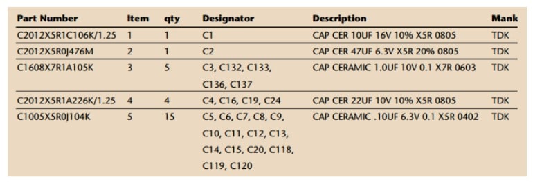
8. Keep your BOM up to date while designing
A bill of material (BOM) is a key aspect of both design and assembly. If there are any issues in your BOM, the assembly house will place the project on hold until the issues have been resolved with an engineer.
One way to make sure your BOM is updated is to review your BOM anytime there is a change in your design. When you add new components to your schematic while the layout is in process, make sure you’ve also updated the BOM with the correct part number, description, and component values.
During the design process, the engineer might change a component due to long lead times, size, or availability and forget to update the BOM with the new part number. This can lead to various assembly issues and cause delays.
Format every bill of materials according to the example below to precisely identify all of the components to be assembled on each board. The properly formatted BOM has columns indicating:
- Full manufacturer’s part number
- Manufacturer’s name
- Item number
- Quantity per board
- Reference designators, separated by commas
- A complete part description
It may also include:
- Distributor’s name
- Distributor’s part number
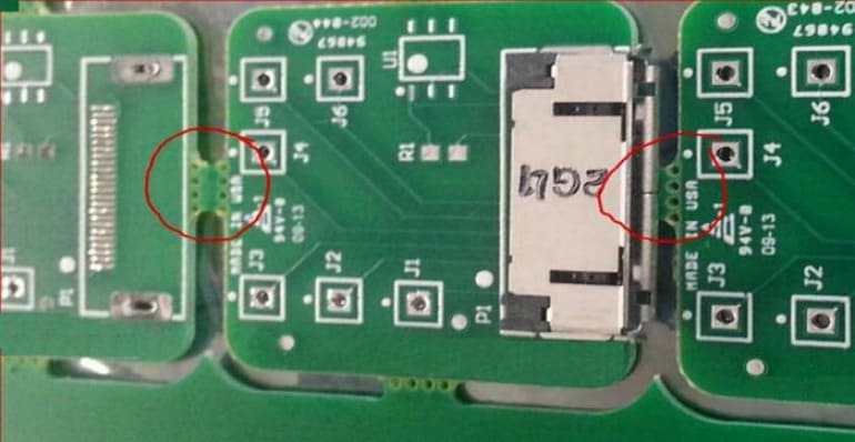
9. Carefully inspect your footprint development
Component footprints are another major aspect of layout design. A PCB Master will make sure their footprints are created accurately as per the land pattern recommended in the datasheet.
It is very important to use the numbering key correctly from the datasheet to identify the correct part and its land pattern.
Reading the datasheet incorrectly will result in an incorrect footprint, which could require a complete redesign and re-fabrication of the boards. To learn more, see our case study, eliminating BOM and footprint errors in PCB assembly.
The image below shows an example of the numbering key and various types of footprints.

Refer to our post on board footprint creation in Allegro, Altium, and KiCad to understand how to design a footprint.
10. Be sure all indicators are present
The leading show-stopper in assembly is missing pin 1 indicators or component polarity/orientation indicators on the silkscreen. Nearly 75% of the assembly orders my facility receives fail to identify the location of pin 1 marking for each IC, or they misrepresent or neglect to indicate the polarity of some capacitors, diodes, or LEDs.

The best way to avoid assembly problems: Confer with your manufacturer before design even begins.
Obey the convention for marking the polarity of diodes, including LEDs: Put a K on the silkscreen layer at the cathode end. Alternatively, use the electrical symbol for diodes in the correct orientation to guide assembly.
Never indicate diode polarity based on the anode pad. Use a K to designate the cathode or line up the diode symbol in the correct position. Don’t substitute any other marks, or your contractor will misinterpret what you intend.
To orient tantalum capacitors, tag the positive side with a plus symbol on the silkscreen. Remember, tantalum capacitors can ignite if mounted with swapped polarity.
Short of reverse-engineering a schematic, there’s no way for a contractor to figure out part polarity unless it’s clearly displayed. Silkscreens must not interfere with pads, and symbols should not be printed beneath the body of any component.
Our article on 6 design mistakes that lead to PCB assembly errors will give you insights into how significant PCBA errors can be avoided by addressing the common design issues.
11. One pad for one connection
Every connection to every component must have its own independent pad. Each pad must be commensurate in size with its mates. If two components share a pad—let’s say, a resistor and a capacitor—neither can be properly aligned during assembly.
And if one pad is substantially larger than its mate for a component, component tombstoning can result from an imbalance of solder deposition.
If a pour or plane will be a point of contact, there must be a mask-defined pad of appropriate size. If a device involves non-solder mask-defined pads for connections as well as solder mask—defined pads, a BGA matrix on a loose pitch in which some adjacent outer balls are common to a ground pour, for example, stipulate in a design note that the board fabricator shall not edit the solder mask apertures for those solder mask-defined pads.
To know about pad design, read What is a Pad in PCB Design and Development?
12. Ease CAM setup
Needless to say, it’s far better to catch issues that might impede assembly before the boards are fabricated. If the board will be fabricated and assembled by the same facility (thereby coordinating operations), verify whether to provide the design data in ODB++ format to speed up identifying potential manufacturing issues and ease CAM setup.
Outputting a design in ODB++ captures the data for fabrication, assembly, and testing in a unified structure that supports automated analysis and avoids time-consuming data conversion at the CAM stage. Practically all major EDA platforms can output design data in the ODB++ format.
13. Address your component delivery
Technically, the 10th tip does not address design but component delivery to the contractor. If assembly will be performed on a consignment basis—some or all of the components will be supplied by the assembly customer, instead of being procured by the assembler—the parts must be provided in a carefully organized kit matching the BOM.
All SMT components must be supplied in reels or on continuous tapes at least 6” in length or in tubes or trays.
Extra components are required for every part number listed on the BOM to cover attrition during assembly. For example, an assembly shop may require a minimum of 100 or 20% more 0201 1k ohm resistors than called for on the BOM.
The parts for each line item on the BOM must be sent in a clearly marked bag separate from the other parts. All ICs must be shipped in their original, unopened protective packages that include desiccant, or else they must be baked for eight hours or so to remove moisture before assembly, which could set back assembly for a day.
In other words, eight strips of eight pieces of a 1005-size 12-pF capacitor do not fulfill a BOM requirement for 64 pieces of that part.
The strips are too short for loading the pick-and-place feeders, and under the best circumstances, not all the parts will wind up on boards. Check and double-check your components before shipping using our kitting guidelines.
We recommend the best way to avoid assembly problems is to consult your manufacturer before the design even begins.
14. Check these additional PCB assembly tips
Additional assembly details to keep in mind during the design stage include heat and wash. Make sure you know what the maximum heat levels of your components are, whether they can be washed, and the type of assembly they require. If it will be hand-soldered, the board design must include space for a soldering tool.
Make sure your capacitors all face the same direction. This saves the pick and place machine time during component placement. Pay attention to components that emit heat. The space around these components must be carefully reviewed. Make sure the heat does not negatively affect any components or traces around the component.
To ensure an error-free PCB assembly, consider our PCB Design for Assembly Checklist: 9 Important Checks for Layout Engineers.
To continue on the path toward becoming a PCB master, keep an eye open for the next piece in the series. If you have any further questions about the board design tips for assembly, please let us know in the comments section. Check out our DFM design guide to learn about design for manufacturing aspects.

Design for Manufacturing Handbook
11 Chapters - 96 Pages - 90 Minute ReadWhat's Inside:
- Annular rings: avoid drill breakouts
- Vias: optimize your design
- Trace width and space: follow the best practices
- Solder mask and silkscreen: get the must-knows
Download Now
Have questions about PCB design for assembly? Post your queries on our forum, SierraConnect. Our PCB experts will answer them.


Start the discussion at sierraconnect.protoexpress.com