


Contents

On-demand webinar
How Good is My Shield? An Introduction to Transfer Impedance and Shielding Effectiveness
by Karen Burnham
Accurate PCB component footprint creation is crucial to ensure precise assembly. Footprint or land pattern is the arrangement of copper pads on which components are assembled.
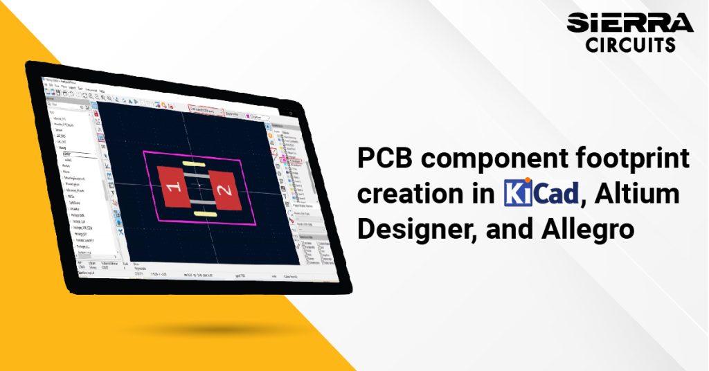
In this tutorial, you will learn how to create a PCB component footprint in KiCad, Allegro, and Altium Designer.
Why create PCB component footprints?
Footprint is a template that guides your manufacturer to assemble the parts on your circuit board accurately. Land patterns for standard parts are generally present in your EDA component library.
However, if you’re using a new component or a modified version of a standard component, you’ll need to create a footprint referring to the datasheet. The footprints should always match the component’s physical dimensions.
The footprints on the board are interconnected using traces and vias. Irrespective of the type of component, be it surface-mount, through-hole, or BGA, there should be a footprint so it can be assembled to the board later.
Key elements of a land pattern
A land pattern gives information regarding:
- Pads/through-holes (pad stack)
- Pin numbers
- Assembly details
- Component centroid
- Pin 1 marking
- Component orientation and polarity
- Component boundary/component keep-out area
- Retaining holes/mounting holes for connectors and special components
- Manufacturer part number
To learn the defects caused by imprecise footprints, see manufacturing defects caused by land patterns.
The standard for creating footprints: IPC-7351
The IPC-7351 depicts the requirements for surface mount designs and land pattern standards. It ensures maximum solder joint quality after the component placement. The solder joint quality should meet the guidelines set by J-STD-001 as well. It also provides guidelines to make space for the components’ inspection, testing, and rework.
A few tips mentioned in this standard are:
- Whenever it is possible to use a common package type, use it. We have options to modify the existing package footprint to suit our requirements.
- A land pattern should only be created from scratch if the package type is not in the library. This process is time-consuming and might lead to errors.
- In addition to IPC standards, consider your manufacturer’s guidelines when it comes to soldering reflow instructions, keep-out areas, courtyards, etc.
- Ensure there is enough space around the component footprint for inspection and rework.
- Incorporate test points for functional tests.
Download our eBook for step-by-step guidance on creating custom libraries and linking symbols to footprints in KiCad 9.

KiCad 9 Step-by-Step Guide
6 Chapters - 41 Pages - 30 Minute ReadWhat's Inside:
- A complete KiCad 9 workflow from project creation to production file generation
- Step-by-step guidance on creating custom libraries and linking symbols to footprints
- Practical design checks: ERC and DRC
- Best practices for generating a clean BOM and fabrication-ready Gerber files
Download Now
How to create a footprint in KiCaD
Before starting the footprint design, gather the necessary specifications of the chosen component.
You need the following details from the datasheet:
- Package type: Identify the package type (SMD or THT). Let us consider the C0603 SMD capacitor as an example.
- Dimensions: Length, width, height, and pad dimensions (L: 1.60 ±10 mm; W: 0.80 ±10 mm; H: 0.80 ±10 mm).
- Pad/lead pitch: Distance between the capacitor’s leads or pads (2 mm).
- Tolerance: Any manufacturing tolerances that might affect the footprint.
- Pad size and shape: Depending on the type of capacitor, pads may be rectangular, oval, or circular. (1 mm x 1.2 mm; rectangular).
- Solder mask and paste mask: Solder mask expansion and paste mask coverage, if required (0 mm).
- Reference designator: The label (e.g., C0603) that identifies the capacitor on the PCB.
Next, if you want to assign a 3D model to the footprint, download the STEP file from the manufacturer’s or supplier’s website.
Follow these steps to create a new land pattern in KiCad:
Step 1: Create a new footprint library.
Open the KiCad tool and select Footprint Editor.

Go to File and New Library. You’ll be prompted with two options: Global or Project.
- Global: Select this if you want the footprint you’re creating to be accessible in all your projects.
- Project: Choose this option if you want the footprint to be available only in your current project
Next, save the new library in the folder of your choice. Make sure the file has a .pretty extension.

Step 2: Add the new footprint to the library.
To create a new footprint, find the newly saved library in the Libraries section, right-click on your library, and choose New Footprint. Next, add the footprint name and type, and hit OK.

Keep these things in mind before you create the footprints:
- When creating footprints, some designers convert component dimensions from millimeters to mil. This increases the risk of pitch measurement errors. Always keep the pitch dimensions in the same units as specified by the manufacturer.
- Pitch measurement is critical for accurate component placement. Changing the units for pitch can lead to significant problems, especially with components having multiple pads in a straight line, such as connectors.
See our tutorial on component placement in KiCad, to learn more.
Before you place a pad, click mm (since the datasheet dimensions are given in mm) to change the dimension from mils to mm, as shown below.

Step 3: Create pads for the component footprint.
- Go to Place in the toolbar and select Add Pad.
- Place the pad as per your requirement, right click on the pad, and hit properties, or double-click to open the pad properties window.

- Here, choose the type of pad (SMD in this case). Pad number, i.e., 1, pad shape is rectangular, pad size X: 1 mm and Y: 1.2 mm.

Step 4: Position the pads.
There are two ways to place pads for accurate positioning:
Method 1:
- Click on Grids in the toolbar.
- Choose 1 mm grid. The component pitch is 2 mm, and the spacing between the origin and the pad should be 1 mm.

- Click and drag the selected pad to the desired location on the grid.
- Ensure that the pad is positioned at the center point of the grid for optimal alignment.

Method 2:
Double click on the pad and input the position parameters in the pad properties dialog. In our case, X is -1, and Y is 0 for pad 1, and then click OK. The pad will automatically snap to the required position. Repeat the same procedure for pad 2. Here, X will be 1, and Y will be 0.

Step 5: Create a component outline.
- To draw an outline of the component body. First, select the F.Fab layer from the appearance section.
- Draw the outline by selecting Add Rectangle option on the right-hand side menu as shown below.
- Draw the rectangle over the pads and right-click and edit the properties.
- Input the start and end point positions. For this capacitor, the values are: start point X: -0.805, Y: -0.405. Endpoint X: 0.805, Y: 0.405.
- Once you enter these values, hit OK. The rectangle automatically positions itself based on the input parameters.

Step 6: Place the component outline on a silkscreen and courtyard layer.
For placing component outline on silkscreen and courtyard, change the units to mil and follow these steps:
- Select the F.Silkscreen layer from the appearance section.
- Add a grid layer of 5 mil.
- Go to Place –> Line (or go to the right-hand side menu and select Add line), draw the silkscreen outlines, right-click, and Edit to change the line width to 5 mils. You can draw the whole outline, but a small outline is sufficient for representation and ensures a minimum clearance of 5 mil from the outermost pad.

- With the same 5 mil grid setting, select the F.Courtyard layer from the appearance section. Draw the outline and ensure a minimum clearance of 15 mil from the pads’ outline.

- Arrange your reference designator; the final component footprint is shown below.

Step 7: Assign a 3D file to the footprint.
- Go to File –> Footprint Properties and then click on 3D Models.
- Upload the STEP file of the component and check the show box.
- Verify if your 3D model has the same orientation as your footprint, and click OK.

- Go to View and click on 3D Viewer to access 3D view of the PCB footprint.

To learn how to create schematic, symbols, and route differential pairs in KiCad, download our eBook.

KiCad Design Guide
10 Chapters - 161 Pages - 180 Minute ReadWhat's Inside:
- Creating a component symbol library
- Setting up board parameters and rules
- How to route differential pairs
- How to place of components
Download Now
How to design a land pattern in Altium Designer®
Let us look at the different steps involved in Altium Designer for PCB component footprint creation. Here, we generate a land pattern for the part number TPD4S014 from Texas Instruments.
Step 1: Go to File –> New –> Library –> PCB library. This will create a new library in which all the new footprints for a particular project will be saved.
Step 2: Check the units in the upper left corner of the window. To change the dimensions, go to View > Toggle units. You can place the pads by clicking on the pad icon in the toolbar (alternatively, Place > Pad).
Step 3: Temporarily place the pad in the middle of the window, then right click –> Properties, and give the required shape and dimensions (x/y). A plated through-hole pad will be created by default, and the hole will be automatically removed when a single-layer pad template is selected.
Step 4: To create multiple pads in an array arrangement, use the paste array option in the top menu. In the new window, give the number of pads and the X-Y spacings needed.
Step 5: The pads are copied and pasted to form the array on the other side. After copying each pad, the properties should be changed as per the datasheet. After placing all the pads, the origin is set from Edit –> Set reference.

Step 6: Draw the component outline on the assembly layer. In Altium, this layer is termed Mechanical 13. Choose the line symbol from the top menu and set the required line width. Here, we are using 4 mil.
Step 7: Add the silkscreen layer next. Under the properties window on the right, choose Top Overlay as the layer and draw the outline to be printed on the silkscreen as shown below.

Step 8: The place-bound layer is termed Mechanical 15 here. Draw the outline by choosing the required line width.
Step 9: Click on the text symbol on the top menu to place the reference designator. It is placed on the Mechanical 13 layer. The properties of the text should be customized using the properties menu.
Step 10: Add Pin 1 marking on the Mechanical 13 layer. This is copied and pasted onto the Top Overlay layer to get printed on the board.
Step 11: Map the 3D package to the footprint by choosing Tools –> Manage 3D bodies for library.
Step 12: Once the 3D package is mapped to the Mechanical 13 layer, the PCB footprint creation is complete.


How to create a footprint in Cadence® Allegro®
Allegro is a flagship PCB editor from Cadence. This design software also offers simple and easy methods for PCB component footprint creation. In this demonstration, we create land patterns for the Murata GCM155R71H104KE02J capacitor.
Step 1: Download the part’s datasheet and understand the dimensions, such as length and thickness.

Step 2: Select the units. Go to Setup –> Design parameters –> Design tab –> User units. Select the unit (here, we choose millimeter) and the tolerance in the accuracy option.

As per the dimensions given in the datasheet, we will draw the assembly outline.
Step 3: Select the required shape from the list of shapes available in the top menu. Here, choose a rectangle.
Step 4: In the options menu on the right, from package geometry, select Assembly_Top as the layer. Under Shape Creation –> Place Rectangle, give the length and width as per the datasheet with the tolerances mentioned.

Step 5: After giving all the dimensions, the required shape will move along with the cursor, which we can place at any location. Move it to the center after placement.
Step 6: Now choose Shape –> Decompose shape, and in the options, under copy to layer, check delete after decomposition and delete existing lines options.
Step 7: Use the lines with 4 mil thickness to accurately draw the package outline in the assembly layer. Select the line option in the shapes menu and change the line thickness to 0.1016mm (4 mils). Then, draw the assembly outline of the package.

Step 8: Add the pads. First, browse the datasheet to see if the pad dimensions are given.

- Open the pad editor and go to File –> New. In the new window, give the name as per convention and choose the pad stack usage as SMD or through-hole. In this case, we are choosing the SMD pin. Select the required pad shape under default pad geometry.

- As the component is SMD, we don’t need to give any details in the drill, secondary drill, drill symbol, and drill offset tabs.
- In the case of through-hole pads, the finished hole diameter with tolerances (depending on plated and non-plated holes) should be given under the drill tab. Under the design layer tab, give the dimensions of the hole pad in the top, internal, and bottom layers. The next tab is the mask layer in which the pad’s Soldermask_Top and Soldermask_Bottom dimensions must be mentioned.
Step 10: Now, back to the SMD pad in hand, go to the design layer –> regular pad –> begin layers (top layer), choose the pad geometry as a rectangle, and enter the dimensions.
Step 11: The same has to be provided in the Mask layer –> Soldermask_Top and Pastemask_Top rows. Check in the summary tab if all the provided data is correct and click save.
Step 12: Close the padstack editor now and return to the PCB footprint creation page. Click Setup –> User preferences and map the created pad stack file path.
Step 13: Insert the pad using the add pin icon on the top menu. In the options, choose the pad, give the pitch (as given in the datasheet), and other details such as the quantity, pin number, rotation, etc.
Step 14: Then place the first pad on the board outline, copy it, and paste it with different pin numbers and rotations for the other pads.

Step 15: For the texts, follow the template, if any, or adjust the text as per the requirements. To change it, go to Setup –> Design parameters –> Text.
Step 16: Add the silkscreen layer. First, select the draw line icon. Go to the options menu on the right side of the screen and select Silkscreen_Top. Then add the required line width for drawing the silkscreen layer. Here, we are adding 0.1524mm (6mils).

Step 17: Now, Add the DFA_Bound_Top layer. In this layer, you need to cover the pad and assembly layers. So, we select a rectangle as the shape and draw a rectangle that covers both the component outer layer and pads.
Step 18: Next, add the Place_Bound_Top layer. We select the layer in the right-hand side menu and give the required offset. This is followed by the addition of the No_Probe_Top layer.

Step 19: Add the reference designator to Assembly_Top and Silkscreen_Top layers. Place the reference designator for the assembly layer inside the land pattern and outside the footprint for silkscreen.

Step 20: Download the 3D version of the package from the repository and map it to the created footprint.
Step 21: Save the footprint as per the IPC naming conventions. Next, go to Tools –> Database, analyze the footprint, and find any errors associated with the creation. In this example, the package didn’t have any pin 1 markings. When packages require pin 1 marking, add it to the silkscreen and assembly layers using the required shape from the menu.
Need help creating accurate PCB footprints for your designs? Our engineering team can assist you with footprint generation, library management, and DFM compliance to ensure seamless manufacturing.
You can book a meeting with our experts or call us at +1 (800) 763-7503.

The PCB component footprint creation is based on the ground rules set by IPC. Different PCB editor tool has slightly different methods for this. Although layers might be named differently in each tool, the basic idea remains the same. Once we understand the general process, it becomes quite simple. PCB where to place a component.
If you have any queries regarding footprint generation. Post them on our forum, SierraConnect; our experts will resolve them.

About Mohamed Faheemuddin : Mohamed Faheemuddin is a mechanical engineer. His passion for electronics drew him to the PCB industry. With an experience of over 3 years in the PCB industry, he specializes in developing articles for engineers and hardware designers.


Start the discussion at sierraconnect.protoexpress.com