


Contents
Crosstalk occurs when high-speed signals from one channel unintentionally interfere with internal/external signals due to fringe electric and magnetic fields. Here, the aggressor signal with a higher amplitude affects the victim trace with less amplitude.
This undesired coupling leads to issues such as voltage overshoot, logic function chaos, and timing delays on PCBs.
In this article, you’ll learn the common reasons for crosstalk occurrence and techniques to eliminate it in your designs.
Highlights:
- Crosstalk occurs due to common impedance coupling and electromagnetic field coupling (capacitive and inductive).
- You can detect crosstalk using oscilloscopes, eye diagrams, TDR, and S-parameter analysis.
- Implement strategies such as 3W spacing between traces, guard traces, and a solid ground plane to prevent crosstalk.
How does crosstalk induce noise in a system?
Crosstalk is categorized into common impedance coupling and electromagnetic field coupling. The common impedance coupling occurs when multiple signals share a common return path. Electromagnetic field coupling is further categorized into capacitive and inductive coupling, which are the most concerning factors.
Every electrical signal has a varied EM field. Whenever these fields overlap, they produce inductive and capacitive coupling. This coupling makes the aggressor signal interfere with the victim signal, even though they are not physically attached but are in close proximity.

Traditional analysis of crosstalk with a pen and paper is not only troublesome but also a time-consuming process. What we can do is estimate the coupling considering the circuit elements. The coupling due to fringe electric fields is approximated by a capacitor (mutual capacitance), and fringe magnetic field-caused coupling is assessed by an inductor (mutual inductance).
Capacitive coupling due to a change in the electric field
Two traces working in parallel on a plane act as parallel plates of a capacitor separated by a dielectric. The change in the electric field between the aggressor and victim is modeled as a capacitor. We know that if there is a voltage change in the capacitor, the electric field changes, and the displacement current is induced. Here, the capacitively coupled current is the crosstalk, and the effect is known as parasitic capacitance.
Inductive coupling through magnetic field rings
Magnetic coupling or inductive coupling is approximated by how many magnetic field rings revolve around the victim trace. The magnetic field change between the aggressor and victim results in a change in the conduction current. Thus, voltage is induced on the victim line as per Faraday’s law of induction. This induced voltage drives the current in the form of crosstalk.
Broadside coupling
Generally, crosstalk happens between two adjacent traces on the same layer. In addition to that, parallel traces separated by a small dielectric contribute to crosstalk. This refers to broadside coupling.

High-Speed PCB Design Guide
8 Chapters - 115 Pages - 150 Minute ReadWhat's Inside:
- Explanations of signal integrity issues
- Understanding transmission lines and controlled impedance
- Selection process of high-speed PCB materials
- High-speed layout guidelines
Download Now
What are the different types of crosstalk?
Here are different types of crosstalk:
Crosstalk categorization based on the signal direction
- Forward crosstalk: It propagates along the direction of the aggressor signal.
- Backward crosstalk: It propagates in the opposite direction of the aggressor signal.

Crosstalk classification by measurement zone
- Near-end crosstalk (NEXT): It refers to the noise on the driver’s side of the victim line.
- Far-end crosstalk (FEXT): It is the disturbance on the receiver side of the victim line.
Crosstalk categorization based on quantification
- Power-sum-NEXT(PS-NEXT): PSNEXT gives total crosstalk from all the adjacent pairs and involves measuring all pair-to-pair groupings relative to power. It is the absolute or relative power of NEXT.
- Power-sum-FEXT (PS-FEXT): PS-FEXT provides you with the absolute or relative power of FEXT.
- Power-sum-equal-level-crosstalk (PS-ELFEXT): It is the sum of PS-NEXT and PS-FEXT.
Alien crosstalk
Here, multiple signals of different frequencies mix with the victim signal, and the situation gets worse when the bandwidth is increased for a faster response. Shielding is not sufficient to prevent this from occurring. You can analyze alien crosstalk using a TDR. For more details, read our post on how TDR impedance measurements work.

Key takeaways:
- Capacitive coupling arises due to changes in the electric field between parallel traces, modeled as a capacitor.
- Inductive coupling involves magnetic field changes around traces, inducing voltage on the victim line per Faraday’s law of induction.
- Forward crosstalk propagates along the direction of the aggressor signal, whereas, backward crosstalk propagates in the opposite.
- NEXT occurs at the driver end, and FEXT is induced at the receiver end of the victim signal.
How to calculate near-end and far-end crosstalk
NEXT is the ratio of the voltage seen on the victim line transmitter end to the voltage that is on the aggressor line.
Our Impedance Calculator uses a 2D field solver to calculate near-end crosstalk based on the following equation:
NEXT = Vb/Va= ¼ (CmL / CL + LmL / LL )
Where,
Vb is the voltage on the driver end of the victim line
Va is the aggressor voltage
CmL is mutual capacitance
LmL is mutual inductance
Far-end crosstalk is the ratio of the voltage on the victim line receiver end to the aggressor voltage. It depends on the propagation delay of the aggressor trace (v), trace length (Len), and the signal rise time(RT), along with mutual capacitance and inductance. Here, Kf is called the FEXT coefficient.
FEXT = Vf/Va = Len/RT ✕ Kf = (Len/RT) ✕ (1/2v) ✕ (CmL / CL – LmL / LL )
Where, Kf = (1/2v) ✕ (CmL / CL – LmL / LL )

How is crosstalk induced in a differential pair?

Whenever there is an imbalance in a differential system, the fields no longer completely cancel and radiate in proportion. Similarly, external fields can induce currents in a differential pair that are not equal in amplitude and opposite in phase. The resultant current is called the common-mode current. Common-mode crosstalk has more adverse effects on the system performance than the differential mode.

How to detect crosstalk in PCB designs
Testing for crosstalk in a PCB design involves using various tools and techniques to measure and analyze the interference between adjacent traces.
Create an eye diagram using an oscilloscope
An oscilloscope can be a valuable tool to identify crosstalk. Here’s how you can use an oscilloscope to detect and analyze crosstalk.
1. Probe placement: Use high-quality probes and connect them to the oscilloscope channels. Place the probes at specific points on the PCB where crosstalk is suspected.
2. Channel configuration: Configure the oscilloscope channels to view the signals from the victim and aggressor traces simultaneously. Assign different colors or styles to easily distinguish between the two signals on the oscilloscope display.
3. Single-ended vs. differential probing: For differential signals, use differential probes to capture the true differential voltage between the two lines. This method provides more accurate measurements for signals that are differentially driven.
4. Eye diagrams: Use the oscilloscope to create eye diagrams for high-speed digital signals. Eye diagrams provide a visual representation of signal quality. Crosstalk can affect the eye pattern, causing it to close partially or completely. A closed-eye pattern indicates poor signal integrity due to crosstalk.
Here’s an infographic that shows how an eye diagram analyzes signal integrity.

Use TDR to identify the impedance discontinuity caused by crosstalk
When the pulse encounters an impedance change caused by crosstalk, part of the pulse reflects back towards the source. These reflections generate spikes on the TDR waveform.

The amplitude of the reflected signal indicates the severity of the crosstalk. Moreover, the time delay between the actual pulse and the reflected one provides information about the location of the crosstalk point from the initial phase. By knowing the signal propagation speed in the transmission line, the physical distance to the crosstalk source can be calculated.
S-parameters
The S-parameters characterize the complex behavior of signals. Each matrix element describes the crosstalk between any pair of ports. They can be measured with a vector network analyzer, as shown in the image.

A 4-port DUT has a total of 16 S-parameters, divided into four quadrants. The parameters in the top right quadrant 2 and bottom left quadrant 3 describe the near-end and far-end coupling of the ports. An unwanted coupling at the near-end of the transmitting port is referred to as near-end cross talk (NEXT) whereas the far-end coupling is known as far-end crosstalk (FEXT).

Referring to the Le Croy signal integrity network analyzer, you can see that even though S31 and S41 measure noise on the same victim caused by the same aggressor, their values differ.
In both cases, the vertical scale is 40db full scale, whereas the horizontal scale for the left one is 1 GHz full scale, and for the right, it is 20 GHz. Also, we can measure S-parameters using a vector network analyzer (VNA). To learn more about this, see s-parameters measurement using a vector network analyzer.

Key takeaways:
- Partial or completely closed-eye diagrams indicate crosstalk and poor signal integrity for high-speed digital signals.
- TDR detects impedance changes caused by crosstalk.
- Determine near-end crosstalk (NEXT) and far-end crosstalk (FEXT) from specific S-parameter elements (e.g., S31 and S41).
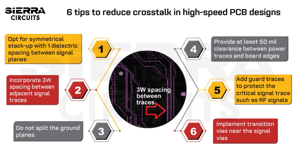
7 design rules to reduce crosstalk in your PCB designs
1. Place the ground plane 1 dielectric away from the signal and power planes
Stick to these design rules when you’re designing your stack-up.
- Arrange the ground plane 1 dielectric away from the signal and power planes.
- Always ensure symmetry of the build-up.
- Keep the power planes sandwiched between two ground planes. This distributes power planes evenly across the stack-up.

2. Ensure optimum spacing between the traces and components
The separation distance between the adjacent traces, as well as between traces and neighboring components, should be large to wipe out the risk of crosstalk. The general rule is separation distance should be equal to 3 times the trace width.

3. Keep signal traces perpendicular to adjacent layers
Arrange PCB layers in such a manner that the traces on adjacent layers are perpendicular to each other, thus preventing broadside coupling. Precisely, we can say that if the traces on one layer follow a north-to-south direction, configure the traces on adjoining layers from east to west.
4. Add guard traces to protect critical signals from crosstalk
Guard traces create a physical separation between the clock trace and adjacent signal traces. They protect the signal line from unwanted electromagnetic coupling and suppress radiated electromagnetic emissions from the clock circuit. Connect guard traces to the ground plane or a dedicated reference voltage. Moreover, provide at least 3W to 5W spacings between the critical traces.

5. Route critical signals on the external layers
Route critical signals such as RF tracks on the external layers. The external layers refer to the top and bottom layers, where components are often placed. Hence, signals don’t have to pass through unnecessary vias, reducing via stub length and the chances of crosstalk.
6. Place the power places at least 50 mil away from the board edges
Placing these planes near the board edges can lead to crosstalk in adjacent layers. Provide at least 50 mil of spacing between the power plane/traces and board edges. Therefore, this space acts as a barrier, minimizing the effects of electromagnetic fields and reducing the risk of interference.

7. Do not split the ground planes
Adhere to these grounding techniques to reduce crosstalk in your designs:
- Keep the return paths and the loop area as small as possible. A smaller loop area means a smaller area through which the changing magnetic fields can couple to nearby traces, minimizing crosstalk and interference.
- Never split the ground planes. Dividing the ground plane can create multiple ground loops, which are paths for stray currents to flow. Ground loops can lead to noise, interference, and erratic behavior in the circuit.

- When there is a change in the reference plane, include transition vias in close proximity to the signal vias. Placing transition vias close to signal vias minimizes the inductance in the return path. A shorter path reduces inductance, ensuring a low-impedance return path for the signal.

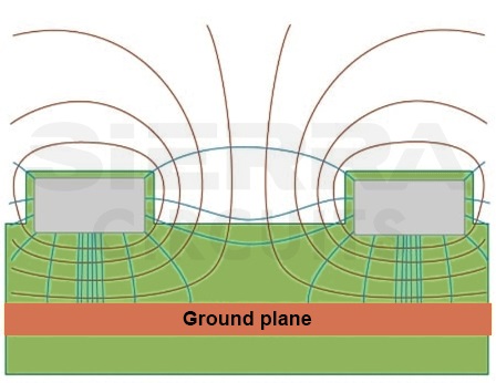
- Create dedicated reference planes for high-speed/critical signals. The solid reference plane absorbs the fringe electric and magnetic fields.
- Cover all unused areas of a circuit with copper pours and connect them to a ground plane.
- Implement via stitching in which multiple vias drill the copper regions on different ground and power planes. This technique enables the shortest return path with the least impedance for multiple layers and minimizes the return loop area. You need to ensure the spacing between vias is at least 1/10th wavelength of the highest frequency you aim to shield.

Key takeaways:
- Arrange ground planes one dielectric away from signal and power planes.
- Maintain a separation distance equal to 3 times the trace width between adjacent traces.
- Introduce guard traces to physically separate critical signals.
- Route important signals like RF tracks on the top and bottom layers.
- Avoid splitting ground planes to prevent ground loops.
- Use transition vias near signal vias to minimize inductance in the return path.
- Implement via stitching with multiple vias drilled in copper regions on different ground and power planes.
Crosstalk in microstrip and striplines
The capacitively coupled current propagates in both clockwise and counterclockwise directions. The current burst in the forward direction incidentally concurs with the aggressor signal. Thus, the far-end crosstalk increases due to capacitive coupling. The backward current dribbles back repeatedly, generating long near-end crosstalk of the same magnitude. Here, in both directions, the voltage pulses are positive.
Inductively coupled current circulates clockwise. The phenomenon in forward and backward is the same as capacitive coupling, except for the fact that here the voltage pulse resulting in far-end crosstalk in the forward direction is negative.

In a stripline, the environment above and below the signal line is homogeneous. Thus, the resulting far-end crosstalk from both couplings will cancel each other out. But in the case of a microstrip line, there is air above the microstrip and dielectric below. This difference in medium causes far-end crosstalk to elevate. Basically dielectric is the reason for electrical coupling. Therefore, we can decrease the capacitive coupling, but far-end crosstalk increases in the case of a microstrip transmission line.
For details, read what is the difference between microstrip and stripline?
PCB Transmission Line eBook
5 Chapters - 20 Pages - 25 Minute Read
What's Inside:
Download Now
Crosstalk can lead to various issues like voltage overshoot, logic disruptions, and timing delays on PCBs. Oscilloscopes, TDR, and S-parameter analysis help detect crosstalk in your PCB design. To mitigate crosstalk, optimize the trace spacing in the circuit, employ guard traces, and ensure proper grounding practices. Additionally, understanding the impact of crosstalk in microstrip and striplines helps in making design decisions to minimize interference and maintain signal integrity.
For techniques to reduce crosstalk in HDI designs, see how to avoid crosstalk in HDI substrate.
If you have any queries specific to signal integrity and crosstalk, post them below. Our experts will be happy to resolve your queries.
About Poulomi Ghosh : Poulomi is a microwave engineer specializing in EMI, EMC, RF, and high-speed electronics. As a senior technical writer at Sierra Circuits, she creates advanced engineering articles and webinars for hardware engineers and PCB designers.


