


Contents

On-demand webinar
How Good is My Shield? An Introduction to Transfer Impedance and Shielding Effectiveness
by Karen Burnham
Surface mount technology (SMT) supports higher component density, short signal paths, and faster automated assembly in modern PCB designs. It helps engineers build compact, high-speed electronic products, but poor SMT layout practices and unreliable solder joints can lead to assembly issues.
As a PCB designer, understanding SMT assembly limitations, component placement, and soldering considerations helps improve reliability and overall circuit performance.
In this article, you’ll learn the advantages and disadvantages of surface mount technology, the differences between SMT and through-hole assembly, and the types of SMD packages.
Highlights:
- Choose SMT assembly if your design has higher routing density, mechanical stress, thermal requirements, and production volume.
- Through-hole technology offers stronger mechanical bonding and is preferred for high-power applications.
- Poor SMT assembly practices can lead to solder joint failures, tombstoning, and solder bridges.
- Proper SMT component placement helps reduce parasitic inductance and improves signal and power integrity.
When was surface mount technology introduced?
Surface mount technology was developed in the 1960s and was used in high-end PCB assemblies during the 1980s and 1990s. It replaced conventional through-hole mounting by allowing components such as metal tabs or end caps to be mounted directly onto the board surface instead of inserting wire leads through drilled holes.
SMT led to much smaller components and enabled component placement on both sides of the board. Surface mounting enables a higher degree of automation, minimizing labor costs and expanding production rates, which results in the development of advanced boards.
What are the features of SMT and through-hole technology?

SMT allows electrical components to be mounted on the board surface without any drilling. Most electronic applications prefer to use surface-mount components since they are compact and may be installed on either side of a printed circuit. They are suitable for applications with higher routing densities. These components have smaller leads or no leads at all and are smaller than through-hole components.
The process involved in SMT assembly is:
- Apply solder paste to the fabricated circuit board using stencils. Solder paste is made up of flux and tin particles.
- Attach the surface-mount components.
- Use a reflow method for soldering.

In through-hole technology, the component leads are inserted into the drilled holes on the board. These leads are then soldered to pads on the opposite side using wave soldering or re-flow soldering tools. Since through-hole mounting offers strong mechanical bonds, it is highly reliable. However, drilling PCBs during production tends to increase manufacturing costs. Also, through-hole technology limits the routing area for signal traces below the top layer of multi-layer PCBs.

Through-hole technology vs. surface mount technology
| Feature | Surface Mount Technology | Through-Hole Technology |
|---|---|---|
| Board space consumption | Low | High |
| Manufacturing cost | Low for high-volume assembly | High due to drilling and manual assembly |
| Design complexity | Requires advanced PCB design and assembly skills | Simpler design and assembly process |
| Pin count | High | Low |
| Assembly process | Supports automated high-speed assembly | Less suitable for full automation |
| Component size | Small | Large |
| Component density | High | Low |
| Equipment investment | High initial investment for SMT machinery | Low machinery investment |
| Typical applications | Compact, lightweight, and high-speed electronic products | High-power, high-voltage, and mechanically robust applications |
| High-speed performance | Better signal performance due to shorter signal paths and fewer holes | Less suitable for high-speed applications |
6 factors to consider before choosing SMT or through-hole technology
PCB designers should evaluate factors such as mechanical stability, thermal management, assembly cost, and rework requirements before selecting SMT or through-hole technology for a design.
Here are a few key factors to consider:
- Stability of the component when exposed to external stress
- Ease of circuit board thermal management
- Availability of the part and its alternative
- Cost-effectiveness of assembly
- High performance and life span of the package
- Facilitate rework in case of board failure
Need help choosing between SMT and through-hole assembly for your PCB design? Our engineering team can help you choose the right technology for your layout.
You can book a meeting with our PCB experts or call us at +1 (800) 763-7503.

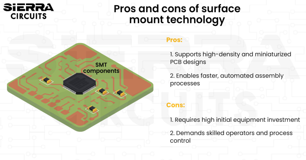
What are the advantages of surface mount technology?
Surface mount technology enables compact, high-density PCB designs with improved high-frequency performance and faster automated assembly. It also reduces manufacturing costs while supporting high-volume production.
Here are the advantages:
- SMDs support microelectronics by allowing more components to be placed closer together on the board. This leads to designs that are more lightweight and compact.
- The process for SMT production setup is faster when compared to through-hole technology. This is because components are mounted using solder paste instead of drilled holes. It saves time and labor-intensive work.

- Components can be placed on both sides of the circuit board, along with a higher component density, with more connections possible per component.
- Due to the compact size of the package, higher-density traces can be accommodated on the same layer.
- The surface tension of molten solder pulls components into alignment with solder pads, which automatically corrects minor placement problems.
- Compared to through holes, these do not expand in size during the operation. Hence, you can reduce the inter-packaging space.
- Electromagnetic compatibility is easily achievable in SMT boards because of their compact package and lower lead inductance.
- SMT enables lower resistance and inductance at the connection. It mitigates the undesired effects of RF signals and provides better high-frequency performance.
- More parts can fit on the board easily due to their compactness, resulting in shorter signal paths. This enhances signal integrity.
- The heat dissipated is also less than that of through-hole components.
- SMT reduces board and material handling costs.
- Enables you to have a controlled manufacturing process. This is especially suited for high-volume PCB production.
Ensure the manufacturability of your circuit design using the Better DFM tool.

What are the disadvantages of surface mount technology?
Surface mount technology can make rework, inspection, and component-level repair more difficult due to smaller package sizes and dense layouts. SMT assemblies are also more susceptible to solder joint reliability issues and require expensive manufacturing and rework equipment.
Other cons include:
- When you subject components to mechanical stress, it is not reliable to use surface mounting as the sole method of attachment to the PCB. This is because you need to use component connectors to interface with external devices that are periodically removed and reattached.
- Solder connections for SMDs might be damaged through thermal cycles during operations.
- You would need highly skilled or expert-level operators and expensive tools for component-level repair and manual prototype assembly. This is because of the smaller sizes and lead spaces.
- Most SMT component packages can’t be installed in sockets that enable easy installation and replacement of failed components.
- When you use less solder for solder joints in SMT, the reliability of solder joints becomes a concern. Void formation might lead to solder joint failures here.
- SMDs are typically smaller than through-hole components, leaving less surface area for marking part IDs and component values. This makes identifying components a challenge during prototyping and repairing the PCB.
- The solder can melt when exposed to intense heat. Therefore, SMT cannot be implemented in electrical load circuits with high heat dissipation.
- PCBs that use this technology require more installation costs. This is because most of the SMT equipment, such as the hot air rework station, pick and place machine, solder paste screen printer, and reflow oven, is expensive.

- Miniaturization and a variety of solder joints can make the procedure and inspection more difficult.
- Due to compact size, there is an increased chance of solder overflow that can result in short circuits and solder bridges.
To learn how to optimize your layout for testing, download the DFT Handbook.
Design for Testing Handbook
7 Chapters - 28 Pages - 45 Minute ReadWhat's Inside:
- PCB testing strategies
- Guidelines to design and place a test point for FPT
- Directives to make your board ICT compatible
- Benefits and drawbacks of various testing methods
- Defects that you can identify through board testing
Download Now
When to use surface mount technology?
You should consider SMT if:
- You need to accommodate a high density of components.
- The need is for a compact or small product.
- Your final product needs to be sleek and light despite component density.
- The requirement specifies the high-speed/frequency functioning of the device.
- You need to produce large quantities with automated technology.
- Your product should produce very little noise (if any at all).
7 guidelines for SMT component placement
Here are seven recommendations for SMD placement to maintain good signal and power integrity for your board.
- Keep the components as close as possible to minimize the routing distance.
- Adhere to the signal path as per the schematic while placing the components.
- Never place the components in the return path of sensitive signals. This leads to signal integrity issues.
- For high-speed devices, place the bypass capacitors closer to their power pins. This will reduce parasitic inductance.
- Arrange the SMDs together for the power supply circuits. This will help you to provide shorter routing and reduce the inductance in the connections.
- Try to keep SMT components on one side of the board to reduce costs associated with stencils and assembly.
- Maintain the minimal spacing between the test points and SMT components as specified by your manufacturer. This spacing may vary depending on the component’s height.

To facilitate the assembly process, ensure that all component names, polarities, orientations, and placements are marked properly in the assembly drawing. The footprints present in the drawings should match the actual parts. Consult your manufacturer for their kitting guideline if you are considering consigned assembly. Prepare your BOM accordingly.
What are the soldering techniques used in assembly?
Solder reflow, wave soldering, and selective soldering are widely used to mount components onto the board. Depending on the nature of the components, the designer can choose one of these methods.

Wave soldering: Since the solder will flow through the holes to form a connection, wave soldering is mostly used for through-hole components. You can use wave soldering for most of the surface-mount components as well.
Selective Soldering: This specialized machine-soldering process is used when a PCB contains delicate components that cannot withstand full-wave soldering.
Solder reflow: This process is generally preferred in SMT. Here, the solder on one pin melts and reflows faster than the other. The only disadvantage is that it causes a tombstoning effect, where the component peels away from the non-melted pad. This effect is common for surface-mount components like resistors, capacitors, and inductors.
What are the types of surface-mount device (SMD) packages?
SMD packages are available in different shapes and sizes, such as passive discrete components, transistors, and integrated circuit (IC) packages.
Let’s look at each of these in detail:
Common passive discrete components: These components are mostly resistors and capacitors and are a part of most electronic devices available today. Given below are the SMD package details for capacitors and resistors.
Transistors: The common types of packages for transistors are as follows:
- SOT-23 (Small Outline Transistor) with dimensions 3 x 1.75 x 1.3mm
- SOT-223 (Small Outline Transistor) with dimensions 6.7 x 3.7 x 1.8 mm

Integrated Circuit (IC) packages
Integrated Circuit packages come in a wide range, as given below:
- Small Outline Integrated Circuit (SOIC)
Small Outline Package (SOP)
TSOP (Thin Small Outline Package) is thinner than SOIC
- Quad Flat Pack (QFP)
Quad flat packs are generic square, flat IC packages.

- Ball Grid Array (BGA)
BGA packages include an arrangement of solder balls on the chip underside in place of pins. The ball spacing typically is 1.27, 0.8, 0.5, 0.4, and 0.35mm

- Plastic Leaded Chip Carrier
The chip is enclosed in a plastic mold. It can either be square or rectangular in shape.
For design for assembly strategies, download the DFA Handbook.

PCB Design for Assembly Handbook
6 Chapters - 50 Pages - 70 Minute ReadWhat's Inside:
- Recommended layout for components
- Common PCB assembly defects
- Factors that impact the cost of the PCB assembly, including:
- Component packages
- Board assembly volumes
Download Now
How are SMD package sizes defined?
SMD package sizes can be defined in inches in the Imperial system and millimeters in the Metric system. For the 0201 imperial components, the dimensions are 0.02 x 0.01 inches. For the 0201 metric components, it is 0.2 x 0.1 mm.
These package dimension standards are specified by the Joint Electron Device Engineering Council (JEDEC) Solid State Technology Association (JEDEC.org). JEDEC is an independent semiconductor engineering trade organization and standardization body that has its headquarters in Arlington, Virginia, United States.
Understanding the advantages and disadvantages of surface mount technology is essential to comprehending its role in the electronics industry. This will always help in optimizing your design and assembly skills. Follow the guidelines listed in this article to completely benefit from the SMT process for component placement.
Need help in designing your PCBs? Post your question on our forum, SierraConnect. Our experts will answer them.

About Sushmitha V : Sushmitha V has a master's degree in power electronics and has over four years of experience in the PCB industry. Her areas of interest include circuit board manufacturing, assembly, IPC standards, and DFM/DFA practices.


Start the discussion at sierraconnect.protoexpress.com