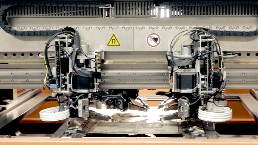
Antipads in PCBs are intentional clearance created on a copper plane to isolate vias from the plane. By managing this copper-free region, you can ensure efficient return paths, minimize parasitic effects, and preserve the overall signal integrity of your circuit board.
Highlights:
- Designing antipads with correct dimensions reduces parasitic effects and improves signal integrity.
- Clearances come in different shapes: circle, oval, and rectangle. Choose the one that best suits your design.
- Always review your fabricator’s drill-to-copper capability before finalizing via-to-plane clearance.
What is the purpose of antipads?
Antipads are created to prevent the via barrel from touching the ground or a power plane as it passes through the stack-up.
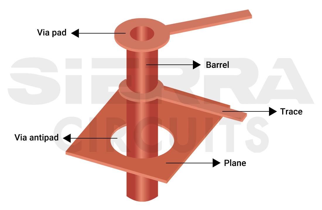
When signal vias pass through internal ground or power planes, the copper around the drill barrel must be removed. Without this clearance, the via barrels would contact the planes and short the signal to ground or power.
How do antipads impact signal integrity?
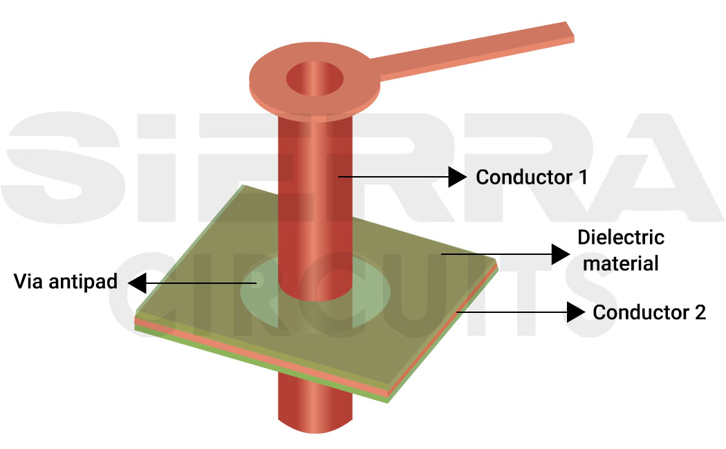
Antipad size directly affects the signal integrity of your board based on the principle of parasitic capacitance. It states that any two conductors separated by an insulator form a capacitor.
Therefore, the via barrel (conductor 1) and the copper plane (conductor 2) form an unintended capacitor and introduce parasitic capacitance.
Therefore, a larger antipad reduces via-to-plane capacitance, improves signal integrity on high-speed signals, and provides cleaner via transitions.
Types of antipads and when to use them
| Antipad type | Description | When to use | When to avoid |
|---|---|---|---|
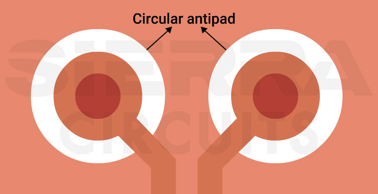 |
A simple round clearance around vias. Gives consistent impedance and predictable parasitics. |
|
|
 |
A clearance stretched in one direction. Lets you route traces through BGAs while keeping good return path continuity. |
|
|
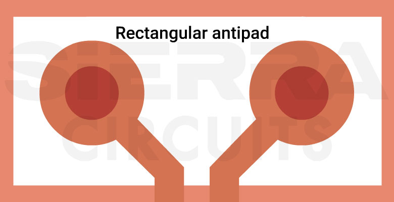 |
A directional opening that shapes fields and reduces coupling along a specific axis. |
|
|
 |
Non-standard geometries (teardrops, or field-solver derived antipad shapes). |
|
|
Sierra Circuits fabricates high-quality circuit boards with precise antipad clearance.
See our rigid PCB manufacturing capabilities to learn more.
5 key factors for designing antipads in your PCBs
When designing antipads, you need to account for via-to-plane isolation, target impedance and geometry, plane integrity and return-path continuity, the fabricator’s drill-to-copper capability, and backdrill depth with residual stub clearance.
Let’s look at each of these in detail:
1. Via-to-plane isolation requirements
Via-to-plane isolation sets the minimum antipad clearance. If this spacing is too small, it can cause unintended contact between the via barrel and the plane. High-voltage and mixed-signal designs require larger isolation to meet creepage and clearance rules.
To ensure consistent isolation, stick to these guidelines:
- Use an identical padstack library so the isolation remains uniform.
- Prefer circular antipads for predictable electromagnetic behavior.
- When implementing oval via-to-plane clearance, ensure it won’t impact impedance or return paths using a field solver.
2. Target impedance and antipad geometry
Via-to-plane clearance directly impacts the parasitic capacitance between the via barrel and plane, which in turn affects impedance. Incorrect dimensions can cause reflections, insertion loss, and degrade high-speed performance.
To maintain uniform impedance, follow these guidelines:
- Run a field solver to confirm pad and via clearance geometry.
- Avoid default libraries for designs that operate above 2.5–5 Gbps; they often undersize antipads.
The following thumb rules can help you select the appropriate antipad size for different design scenarios:
| Design scenario | Thumb rules |
|---|---|
| High-speed signal vias | Antipad ≈ finished hole + 20 mil (or pad diameter + 12 mil) |
| Standard thermal relief spokes | Antipad = pad diameter + 10 mil |
| Via protection as per IPC-4761 | Antipad = finished hole + 16 mil Thermal relief web = 8 mil |
| Generic clearance as per IPC-2221 | Antipad ≥ finished hole + 20 mil (10 mil radial clearance) |
Use Sierra Circuits’ Via Impedance Calculator to calculate impedance, capacitance, and inductance of your plated holes.
3. Reference plane integrity and return-path continuity
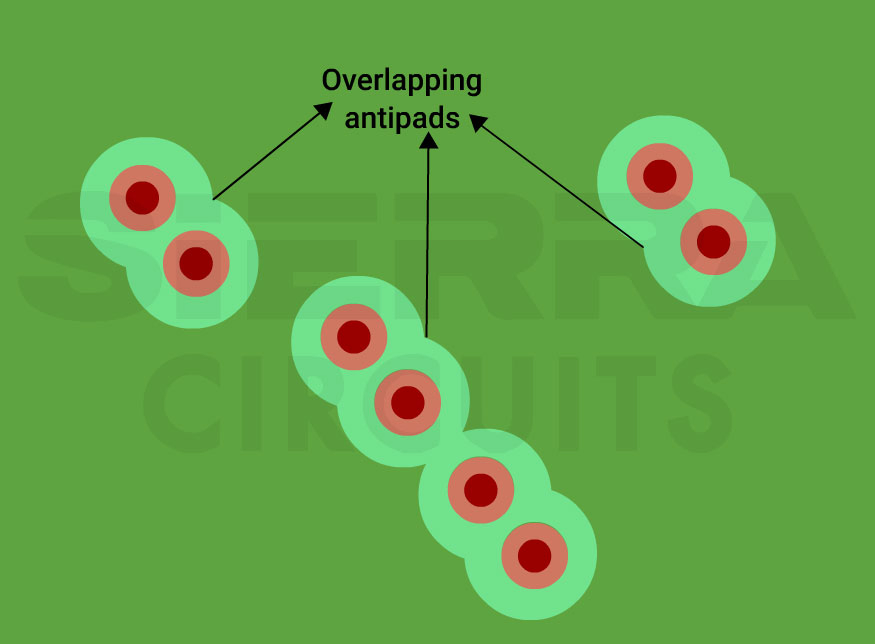
Tightly grouped vias can cause antipads to merge on internal planes. When multiple vias transition through different layers in the same region, their via-to-plane clearance may overlap and create slots (voids) in the reference plane. These voids disrupt return paths, increase loop inductance, and can elevate EMI.
To maintain reference plane integrity and preserve return-path continuity, follow these best practices:
- Space vias based on antipad diameter.
- Stagger layer transitions when routing DDR and PCIe to avoid clustering antipads in a single zone.`
- Use stitching vias or short copper bridges to reconnect the return-current path around unavoidable voids.
- Define no-via zones for sensitive plane regions such as analog grounds or high-speed reference planes.
- Place high-speed decoupling capacitors away from dense via clusters to reduce the return path loop.
Overlapping via spacing in a PCB layout.
4. Drill-to-copper capability of the fabricator
The manufacturer’s drill-to-copper capability determines the optimum via-to-plane clearance for your PCB. Drill wander, tool runout, and plating tolerance can shift the finished hole toward the plane, reducing clearance and increasing the risk of shorts.
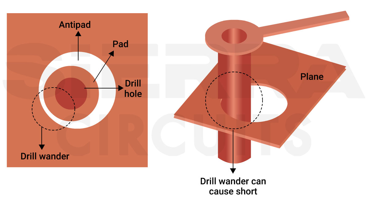
To account for drill variation and ensure adequate clearance, follow these guidelines:
- Finalize the clearance based on the fabricator’s drill-to-copper specification (8–10 mil typical).
- Increase the via-to-plane clearance diameter when using thicker copper, as drill wander increases with copper weight.
- Consult your fabricator for layer-specific drill-to-copper tables, especially for class 3 designs.
5. Backdrill depth and residual stub clearance
Backdrilling uses a larger drill bit, so antipads on the backdrilled layers must accommodate the bigger tool diameter and tolerance. Even when the stub is removed, the backdrill barrel still passes near internal copper, requiring larger clearance.
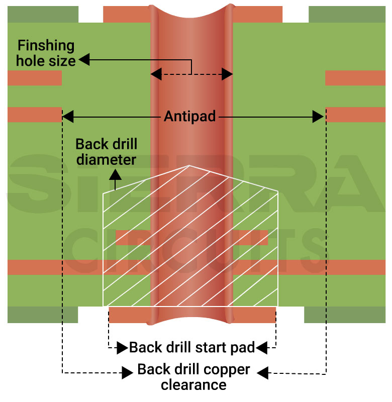
To ensure backdrill compatibility and prevent residual stub issues, follow these guidelines:
- Specify backdrill depth and tool size in fabrication notes.
- Increase the clearance on all backdrilled layers by tool radius + tolerance.
- Get the CAM team’s feedback to confirm backdrill compatibility.
For more tips, download the PCB Via Design Guide.
PCB Via Design Guide
7 Chapters - 90 Pages - 70 Minute ReadWhat's Inside:
- Guidelines for choosing the right via for your application
- Design rules for advanced via structures
- DFM tips to avoid manufacturing errors
- Signal integrity considerations for high-speed designs
- Testing and inspection methods for via reliability
- Fab notes
Download Now
Things to include in your fab notes about antipads
- Antipad definitions: Clearly define all antipad requirements in the padstack library and fabrication notes.
- Pad and antipad dimensions: Specify pad and antipad diameters for every via type.
- Drill information: Include finished drill size, drill tolerance, backdrill depth, and drill-to-copper clearance.
- Layer-specific antipads: Provide layer-specific via-to-plane clearance values for controlled-impedance vias or backdrilled vias.
Antipads play a crucial role in maintaining the signal integrity of high-speed printed boards. Always discuss with your CM before finalizing the clearance values to prevent delays. In addition, clearly mention your requirements in the fabrication notes.
